
A PTFE board can be electrically well designed and still be difficult to quote or panelize. The manufacturing risk is concentrated at the interfaces: copper balance, drilled features, plated edges, hybrid stackup boundaries, connector rails, and the coupon that is supposed to represent the RF path. A PTFE PCB release should therefore explain the process assumptions that keep the first panel comparable with the final product.
Panelize for RF and process stability
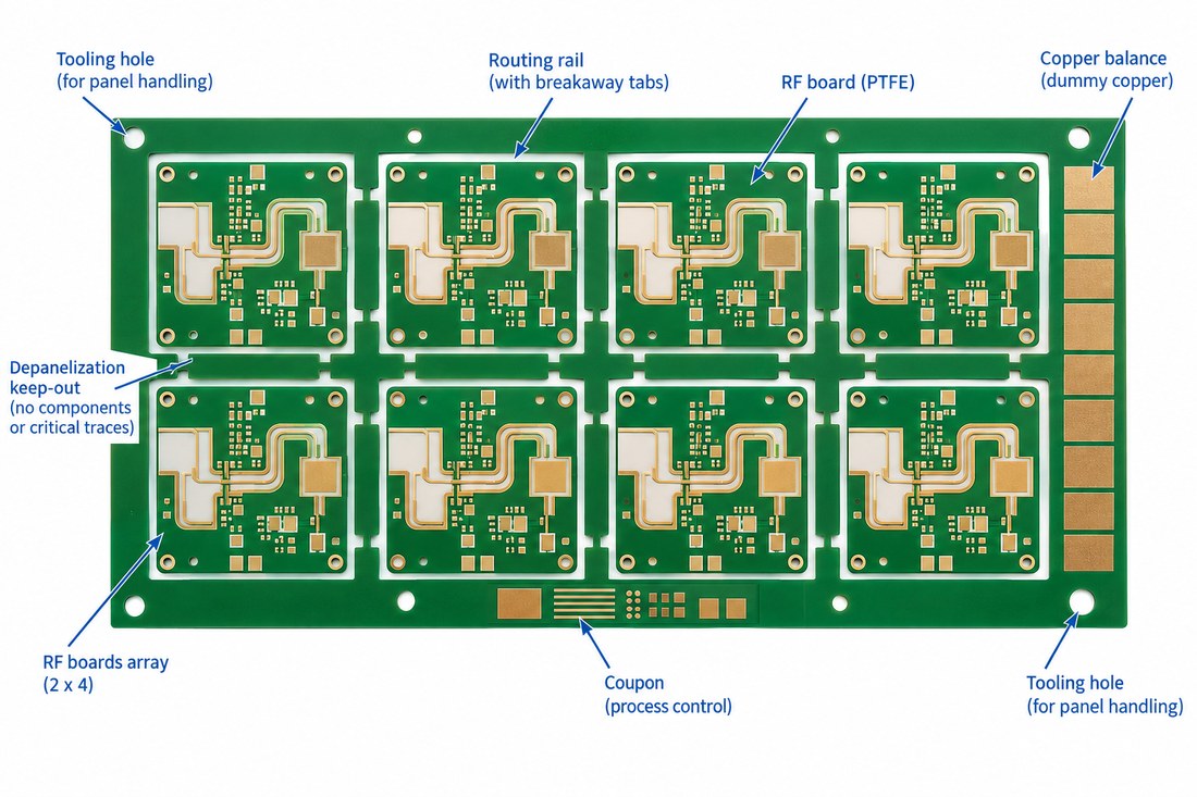
Place RF features, thermal features, and tooling in a panel that supports the actual process route. The PTFE PCB panel drawing should show orientation, rails, fiducials, breakaway method, copper thieving, and the location of any controlled-impedance coupon. Avoid placing a sensitive launch next to a rail or heavy copper area without checking the local etch and plating effects.
Balance large copper areas and isolated planes where practical. The RF PCB manufacturing review should also identify whether the panel will be drilled, routed, or scored, because the edge method can change the connector datum and create burrs near the RF region.
If the product combines PTFE and FR-4 sections, show the boundary and lamination sequence. Treat the transition as an electrical and mechanical feature, not a note hidden in the material list.
Protect the material specification
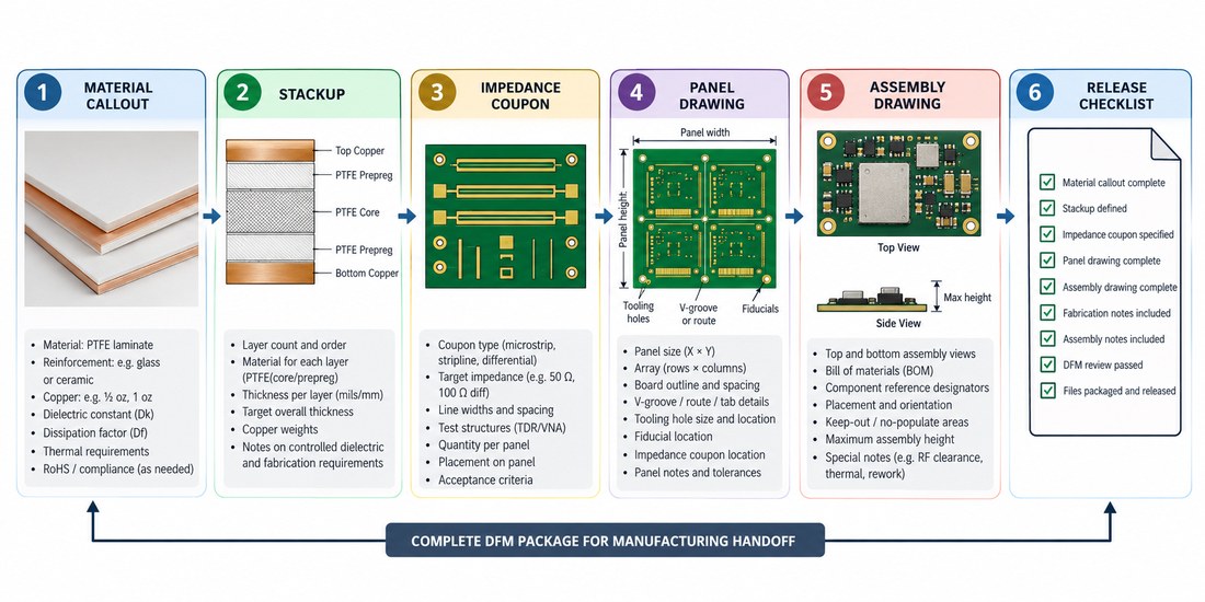
List the approved PTFE construction, copper foil or treatment, finished thickness, surface finish, and acceptable alternate process. A PTFE PCB with a similar nominal Dk can still have different loss or etch behavior if the copper and reinforcement change.
The controlled impedance procurement note should reference the exact supplier data sheet revision and identify which values are typical. If a substitute is proposed, require a stackup review, impedance recalculation, and a decision on whether a new coupon is needed.
Keep material, stackup, and panel revisions synchronized. A purchase order that calls out only “PTFE PCB” leaves too much room for an unintended construction.
Create a handoff that survives ECOs
The release package should include fabrication drawing, stackup, drill table, panel, impedance coupon, assembly drawing, and inspection plan. The thermal management checklist should name the owner for any deviation and the latest revision of the connector footprint.
When a design change moves a line or changes copper density, recheck the coupon and panel position. A drawing revision without a panel revision can invalidate the process evidence.
Use a pre-production review with design, manufacturing, assembly, and procurement. The goal is not to promise an unsupported result; it is to make every assumption visible before the first panel is ordered.
PTFE PCB DFM is a coordination task. A stable panel, precise material callout, representative coupon, and synchronized ECO process make the RF design easier to build and easier to defend.
Implementation note for this DFM and procurement release review: keep the engineering assumption visible at the point where it affects a drawing, a supplier quote, or an inspection record. Ask the design owner to identify the reference plane, interface datum, and acceptance method before the release is frozen. Ask manufacturing to return the proposed stack, panel, and process window rather than a generic capability statement. Ask assembly to identify the profile, cleaning, and support conditions that could move the RF or thermal result. This simple handoff prevents a typical material value from being mistaken for a guaranteed product result and gives the project team a clear action when an ECO changes the physical boundary.
Release note: keep the PTFE PCB panel drawing, material callout, and inspection plan under the same revision so repeat builds use the same manufacturing assumptions.
Sources: Panasonic MEGTRON technical material guidance; Rogers and Taconic high-frequency material data sheets where relevant; CeramTec ceramic substrate data; Analog Devices RF and mixed-signal layout guidance. Numerical values are treated as typical supplier values or engineering targets unless the released drawing defines a measured acceptance value.
Release note: confirm the PTFE PCB construction before the next ECO.
Release note: confirm the PTFE PCB construction before the next ECO.
Release note: confirm the PCB manufacturing evidence before approval.
Release note: confirm the PCB assembly evidence before approval.
