
Ceramic PCB programs often move from concept to purchase order faster than the manufacturing package matures. The layout may be complete, but the supplier still lacks a defined panel, edge condition, metallization note, inspection plan, or approved substitute rule. That gap creates schedule risk because a ceramic panel is not interchangeable with a conventional laminate panel. A Ceramic PCB release should therefore be treated as a manufacturing contract as well as an electrical design.
Turn the drawing into a process conversation
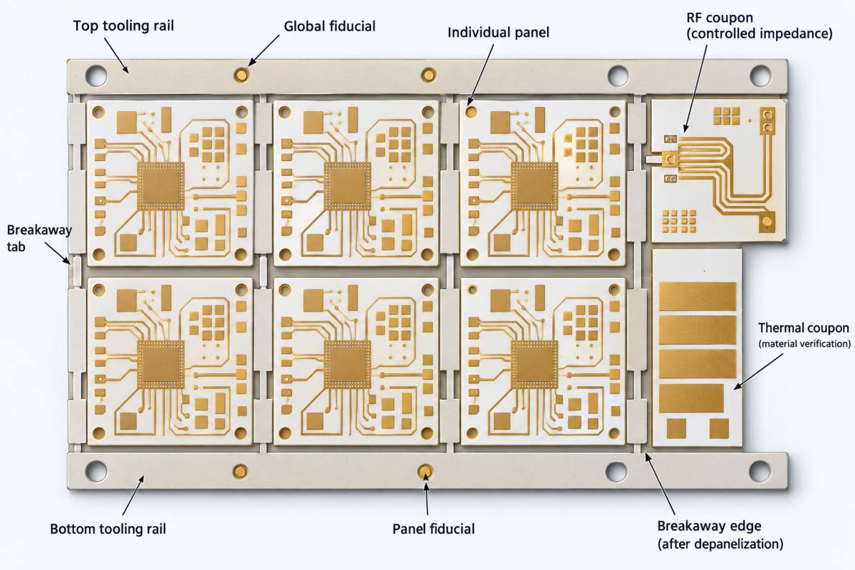
Start with a feature list: substrate size, thickness, copper system, conductor width and spacing, via technology, cavities, fiducials, tooling holes, and edge clearance. The Ceramic PCB drawing should identify which dimensions are electrical, mechanical, or cosmetic. This lets the fabricator quote the correct process instead of applying a generic PCB rule set.
Ask for a proposed panelization drawing before the purchase order is frozen. Show the material grain or orientation if relevant, the handling frame, sacrificial rails, breakaway method, and the locations of RF and thermal coupons. The RF PCB review should also cover whether the panel can pass through plating, imaging, inspection, and assembly without unsupported edges.
If the design uses a carrier or metal-backed assembly, include the carrier drawing in the same review. A ceramic board can meet the drawing while the combined stack fails flatness or connector coplanarity.
Control the first article evidence
Define the cross-section plan before fabrication. Identify the locations that prove copper thickness, via fill or plating, ceramic thickness, cavity depth, and the interface to the carrier. The Ceramic PCB lot should not be accepted from a photograph alone when the critical feature is internal.
The controlled impedance handoff should separate process capability information from lot acceptance. A supplier may provide a typical capability window, while the project may need a specific dimensional record for each lot. Keep both statements visible so procurement does not accidentally turn a typical value into a contractual guarantee.
For RF boards, include a coupon or witness feature only when it represents the production geometry. A generic coupon can be useful for process monitoring but cannot prove a narrow antenna launch or cavity wall without correlation.
Close substitutions and ECOs before release
Ceramic families can look similar on a material list while differing in shrinkage, metallization, thermal behavior, or available thickness. The thermal management purchasing note should list the approved material identifier, supplier, revision, and the review required for any alternate.
When an ECO changes pad size, cavity depth, connector position, or mounting hole, route it through RF, mechanical, manufacturing, and assembly owners. Reuse of a previous drawing number is risky if the ceramic panel or tooling has changed.
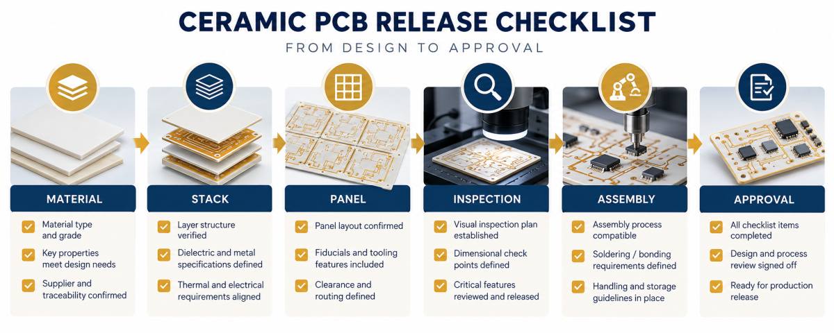
Use a final release checklist: verified stack and material, panel drawing, datums, inspection plan, approved finish, assembly notes, shipment packaging, and deviation owner. That checklist lets KKPCB coordinate the build without implying an unsupported customer result.
Ceramic PCB DFM is successful when procurement, manufacturing, RF design, and assembly see the same constraints. A clear panel and evidence plan prevents a technically correct layout from becoming an unbuildable purchase order.
Implementation note for this DFM, procurement, and project release review: keep the engineering assumption visible at the point where it affects a drawing, a supplier quote, or an inspection record. Ask the design owner to identify the reference plane, interface datum, and acceptance method before the release is frozen. Ask manufacturing to return the proposed stack, panel, and process window rather than a generic capability statement. Ask assembly to identify the profile, cleaning, and support conditions that could move the RF or thermal result. This simple handoff prevents a typical material value from being mistaken for a guaranteed product result and gives the project team a clear action when an ECO changes the physical boundary.
Sources: Panasonic MEGTRON technical material guidance; Rogers and Taconic high-frequency material data sheets where relevant; CeramTec ceramic substrate data; Analog Devices RF and mixed-signal layout guidance. Numerical values are treated as typical supplier values or engineering targets unless the released drawing defines a measured acceptance value.
Release note: confirm the Ceramic PCB construction before the next ECO.
Release note: confirm the Ceramic PCB construction before the next ECO.
Release note: confirm the PCB manufacturing evidence before approval.
Release note: confirm the PCB assembly evidence before approval.
