
Outdoor radar and sensor hardware sees temperature swings, condensation risk, vibration, and repeated enclosure loads. A Ceramic PCB can reduce some dimensional and moisture-related uncertainty, but it does not remove the need to coordinate the ceramic, copper, seal, connector, and metal housing. The project pain appears when a material is chosen for a nominal dielectric value while the assembly still has a mismatch in CTE or an unqualified seal path.
Table of Contents
- Define the environmental boundary before selecting the stack
- Protect the RF path while managing seals
- Make the environmental release auditable
Define the environmental boundary before selecting the stack
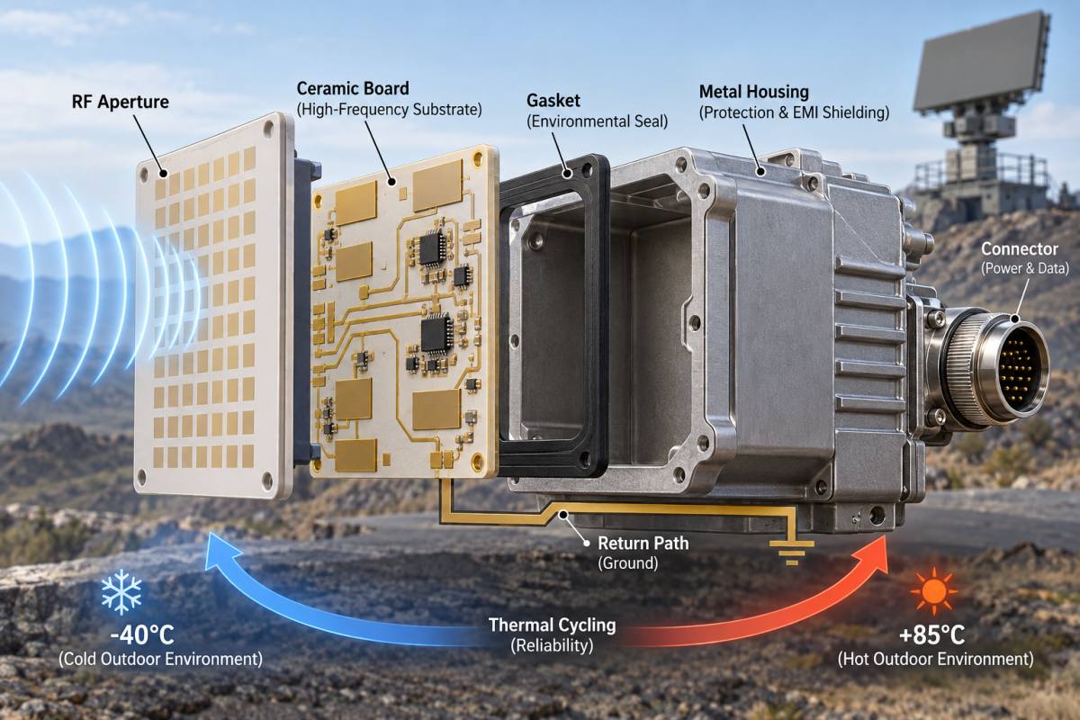
List the real exposures: storage humidity, operating temperature, cycling rate, salt or dust, vibration, and the enclosure pressure path. The Ceramic PCB material data should be reviewed against these exposures, but the final requirement belongs to the complete module. A ceramic substrate may have low moisture uptake while an adhesive, solder mask, connector gasket, or cable entry does not.
Create a CTE map for the substrate, copper, carrier, housing, and fasteners. A small mismatch can be acceptable when the interface is compliant; a large mismatch becomes a fatigue risk when the ceramic is clamped across a wide span. The RF PCB design review should show the neutral axis, fastener pattern, and any edge that is constrained by a seal.
For a radar front end, keep the antenna aperture and connector datum separate from the housing datum until the mechanical tolerance stack has been closed. Do not hide a dimensional correction in a last-minute CAD offset because it will be lost when the panel drawing is regenerated.
Protect the RF path while managing seals
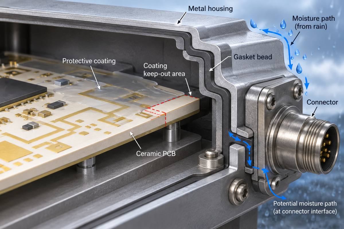
A seal or coating can change the local dielectric environment around an antenna, cavity, or launch. The Ceramic PCB keep-out should identify the permitted seal bead, adhesive fillet, and coating thickness. If the seal is close to a controlled line, define the maximum intrusion rather than saying “avoid RF area.”
Use a continuous return path around the connector and shield boundary. The controlled impedance layout must account for mounting holes and gasket gaps so they do not become unintended slots. If a ground fence is interrupted, document the electrical reason and the alternate return route.
A qualification fixture should represent the final housing and seal stack. A board-only test can establish a baseline, but it cannot prove the environmental configuration unless the enclosure, torque, and gasket are included.
Make the environmental release auditable
Separate typical material values, design targets, and measured acceptance values in the build documentation. The thermal management package should include the thermal-cycle profile, inspection locations, seal inspection, and any RF retest required after cycling. Keep the acceptance language tied to the product requirement rather than an arbitrary number copied from a different assembly.
If the ceramic supplier changes metallization or the housing supplier changes a coating, trigger a joint review. Revisit RF clearance, CTE assumptions, seal compression, and cleaning compatibility. A change-control note that only says “same material family” is not enough for an outdoor module.
Close the project gate with a single page: environmental boundary, datum scheme, seal keep-outs, return path, inspection evidence, and the owner for deviations. That format helps the project manager see which risks are still engineering actions and which are already accepted.
A Ceramic PCB is an enabler for harsh-environment RF hardware, not a waiver from environmental engineering. Release the substrate together with the housing, seal, return path, and inspection evidence so field reliability is designed rather than assumed.
Implementation note for this harsh environment and dimensional stability review: keep the engineering assumption visible at the point where it affects a drawing, a supplier quote, or an inspection record. Ask the design owner to identify the reference plane, interface datum, and acceptance method before the release is frozen. Ask manufacturing to return the proposed stack, panel, and process window rather than a generic capability statement. Ask assembly to identify the profile, cleaning, and support conditions that could move the RF or thermal result. This simple handoff prevents a typical material value from being mistaken for a guaranteed product result and gives the project team a clear action when an ECO changes the physical boundary.
For this outdoor Ceramic PCB module, keep the environmental boundary visible in the drawing so the seal, housing, and return-path decisions remain traceable through an ECO.
The Ceramic PCB CTE review should include the housing, seal, connector, and carrier rather than treating the ceramic substrate as an isolated value.
A second Ceramic PCB CTE review should connect the substrate assumption to the housing, gasket, and connector support used during qualification.
Sources: Panasonic MEGTRON technical material guidance; Rogers and Taconic high-frequency material data sheets where relevant; CeramTec ceramic substrate data; Analog Devices RF and mixed-signal layout guidance. Numerical values are treated as typical supplier values or engineering targets unless the released drawing defines a measured acceptance value.
Release note: confirm the Ceramic PCB construction before the next ECO.
Release note: confirm the Ceramic PCB construction before the next ECO.
Release note: confirm the PCB manufacturing evidence before approval.
Release note: confirm the PCB assembly evidence before approval.
