
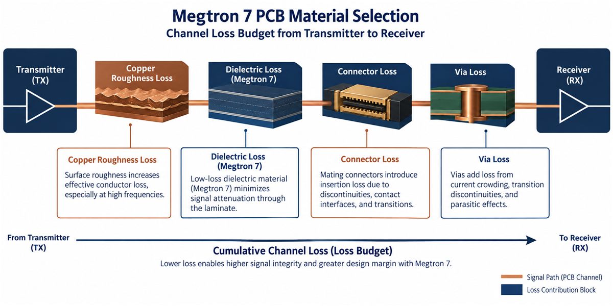
A long backplane channel can fail a design review even when the laminate choice looks correct on paper. The usual problem is not one dramatic defect; it is the accumulation of copper profile loss, dielectric loss, connector discontinuity, via loss, and local glass-weave skew. A useful Megtron 7 PCB project therefore starts with a channel budget that the fabricator can actually build and inspect.
Start with a channel loss budget
Panasonic lists MEGTRON 7 families such as R-5785(N), R-5785(GN), and R-5785(GE) for high-speed, large-format multilayer boards. Typical published values include a Tg around 200 °C, T288 with copper above 120 minutes, and low Dk/Df values that vary by grade and test method. Those are material reference values, not a guaranteed channel result. The project team still has to allocate loss between trace length, copper treatment, connectors, and transitions.
At the architecture stage, separate the channel into straight transmission line, breakout, connector launch, via field, and package sections. Give each section a working allowance and identify which allowance is a design target rather than a measured result. This makes a change in board thickness or connector part visible before layout is frozen. A Megtron 7 PCB should also state the selected glass style, resin content range, copper foil family, and the frequency used for the electrical model.
Control copper profile and glass-weave effects
At multi-gigabit edge rates, conductor roughness changes the effective current path and can consume margin that was assigned to the dielectric. Specify the copper treatment and the side of the foil used for critical outer-layer or stripline routes. Keep the rule tied to the actual stackup rather than writing a generic “smooth copper” note that production cannot verify.
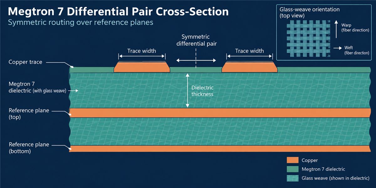
Glass weave is a different risk. A differential pair that runs beside a resin-rich window can see a different local effective permittivity from a pair crossing a dense glass bundle. The resulting delay difference appears as skew or phase error. Use route spreading, small pair-angle changes, and weave-aware breakout rules where the channel length makes the effect meaningful. Avoid an arbitrary serpentine correction: it may add coupling without correcting the local dielectric environment. The controlled-impedance PCB layout process should include the pair reference planes, allowable skew, and the point at which a trace must be re-simulated.
Convert the review into a release package
A production-ready release package names the controlled dimensions: dielectric thickness after press, finished copper, trace width and spacing, back-drill assumptions, and coupon geometry. It also identifies what the coupon represents. A coupon built on an isolated test line cannot automatically prove the loss of a connector launch in the product channel.
For project managers, the practical checkpoint is a red-line list: any material substitution, foil change, resin-content change, or layer move must trigger an impedance and skew review. KKPCB can align the Megtron 7 PCB with the released stackup, while the high-frequency PCB capability team checks the RF-critical geometry. If the product includes dense press-fit or high-speed connectors, route the final decision through PCB assembly planning and confirm that the connector footprint remains compatible with the fabrication datum.
Before sign-off, verify five items: the grade and glass style are named, copper profile is controlled, weave-sensitive pairs are identified, coupons represent the real construction, and ECO rules protect the loss budget. This disciplined sequence lets a Megtron 7 PCB preserve signal margin without pretending that a typical material value is a customer measurement.
Use a assembly inspection plan and a via-transition capability review before sign-off.
Verify the Megtron 7 PCB assembly datum before release.
Sources: Panasonic Industrial Devices MEGTRON 7 series page and published R-5785/R-5680 data; KKPCB PCB Materials and high-frequency capability pages. Numerical values above are typical manufacturer values or design-review targets, not KKPCB customer measurements.
