
The controlled Megtron 6 PCB datum should be reviewed before thermal cycling begins.
For a dense compute Megtron 6 PCB, copper balance and registration targets belong in the same release package.
A second Megtron 6 PCB construction should never be approved without a revised coupon plan.
Megtron 6 PCB thermal reliability is a registration problem as much as it is a material problem. Dense compute, networking, and accelerator boards move through lamination, reflow, power cycling, and environmental storage while copper, dielectric, solder mask, connectors, and components expand at different rates. If the project team treats thermal cycling as a final test only, the registration drift has already been built into the design. This guide connects material data, stackup decisions, fabrication controls, and release evidence.
Table of Contents
- Where registration moves
- Stackup and copper controls
- Thermal cycling evidence
- Production release checklist
Where thermal registration moves in a multilayer board
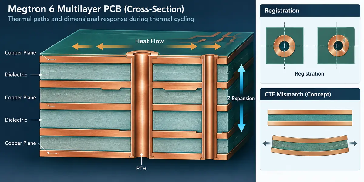
A multilayer panel is exposed to heat during press cycles, copper plating, solder-mask cure, and assembly reflow. The board does not expand uniformly because copper patterns, resin content, glass style, and local heat paths are different from area to area. The relevant question for a Megtron 6 PCB is not only its glass-transition temperature; it is whether the finished construction keeps holes, pads, differential pairs, and connector datums inside the same positional window after the complete process sequence.
Panasonic MEGTRON 6 family data provides typical Tg, Td, CTE, Dk, and Df values for named constructions. Use the exact grade and test method from the selected data sheet, then ask the fabricator to convert those values into a finished stackup and process plan. Do not use a family-level value as a guaranteed board-level measurement.
Build the stackup around thermal symmetry
Balance copper and dielectric
Uneven copper loading creates a different thermal response on each side of the panel. Large planes beside sparse routing, heavy connector fields, or copper pours that stop at a keep-out can pull registration during pressing and plating. The high-speed PCB manufacturing review should compare copper distribution by layer, not only the final Gerber image. Add balancing copper where it does not affect impedance, creepage, antenna clearance, or thermal isolation.
Dielectric thickness also changes when resin flows around dense copper. A Megtron 6 PCB stackup should define finished dielectric targets, glass style, pressed thickness, and the tolerance used for impedance calculations. When the design includes thin cores, sequential lamination, or high layer count, place registration targets near the features that matter rather than relying on a single panel datum.
Protect reference planes and critical datums
Keep differential pairs, connector launches, and fine-pitch escape routes referenced to continuous planes. Plane splits and large resin windows can change local stress and make the electrical path sensitive to small shifts. The PCB layout review should overlay critical holes, pads, and pair transitions against the mechanical datum and the expected press direction. The Megtron 6 materials page confirms the intended family, while the released drawing controls the actual construction.
Use coupons to separate material behavior from process drift
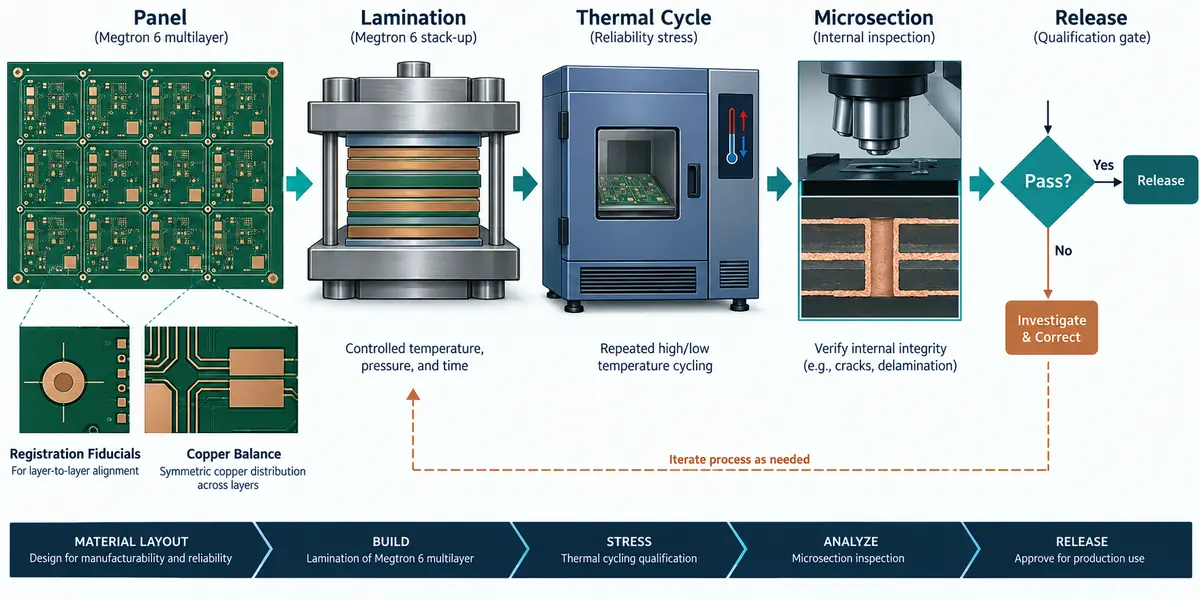
A thermal coupon should answer a specific question: did the material and process keep the feature within the release window after conditioning? Select coupons that represent the product’s layer count, via structure, copper distribution, and registration-sensitive features. Record the conditioning sequence, measurement datum, and acceptance range. A coupon that uses a different glass style or a light copper pattern can produce a clean result while missing the product risk.
For a dense Megtron 6 PCB, combine cross-section evidence with dimensional checks at the connector, BGA, and via fields. A cross-section can verify dielectric thickness, copper balance, plated-hole quality, and resin fill. Dimensional inspection can confirm that the electrical path and mechanical datums remain aligned after the thermal cycle. These are engineering release checks, not a claim of a customer measurement.
Coordinate assembly and change control
Reflow adds another thermal exposure and can reveal a registration issue that was not visible on bare boards. Solder-mask expansion, paste aperture, connector coplanarity, and component keep-outs should be reviewed against the same datums used in fabrication. The PCB assembly plan should state how board support, profile windows, and inspection references protect the launch and fine-pitch escape.
For early builds, PCB prototype assembly helps expose thermal-mechanical interactions before volume tooling is fixed. If a supplier proposes a different press cycle, copper foil, or surface finish, route the change through the same stackup and registration review. Do not close the engineering change on price and lead time alone.
Project release checklist
- Exact laminate grade, glass style, finished dielectric, and test method recorded.
- Copper balance reviewed by layer and by panel quadrant.
- Registration datums placed near connector, BGA, via, and impedance-critical features.
- Thermal coupon construction represents the product stackup and copper pattern.
- Conditioning sequence, dimensional method, cross-section plan, and acceptance window defined.
- Assembly reflow and component keep-outs tied to the same mechanical datum.
When a project manager needs a defensible release, the Megtron 6 PCB layer map, the Megtron 6 PCB fabrication notes, and the Megtron 6 PCB assembly constraints should be revised together. That simple discipline keeps thermal registration from becoming a late yield surprise.
Sources: Panasonic Industrial Devices MEGTRON 6 family and R-5775/R-5670 technical data; supporting thermal and high-speed layout guidance from Analog Devices and Qorvo application material; KKPCB verified pages for manufacturing, layout, assembly, prototype assembly, and MEGTRON 6 material capability. Values are typical or design-reference values unless a released drawing defines the acceptance limit.
