
Taconic RF-35 PCB coupled-line filter performance is governed by geometry that fabrication can actually hold. The filter designer may calculate a narrow gap and exact line length, but etch bias, copper profile, dielectric thickness, plating, and solder mask decide whether the finished board has the intended coupling. That is why a filter release needs more than a schematic and nominal laminate callout.
Table of Contents
Translate filter equations into finished geometry
Start from finished trace width, gap, copper thickness, and reference-plane spacing. Taconic RF-35 PCB line dimensions should include the expected etch and plating condition, not just the CAD artwork. The RF PCB design RF PCB design review should show which dimensions dominate coupling and which are safe to leave at a broader process tolerance.
Protect the coupled-line edge environment
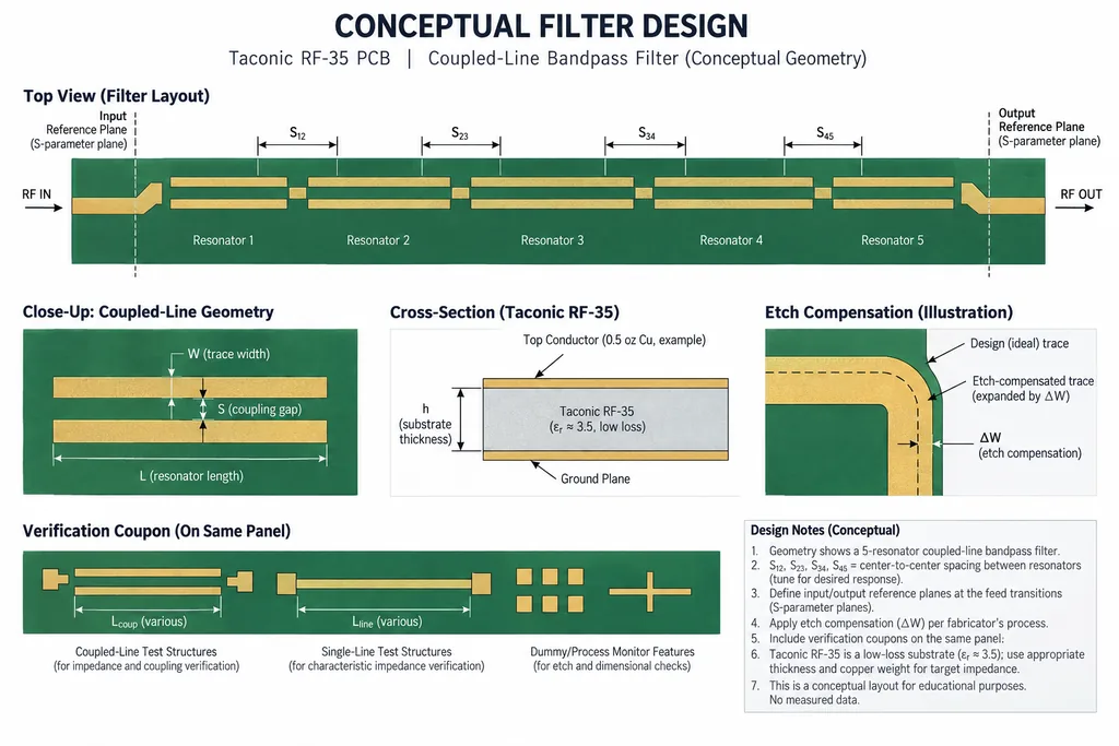
Solder mask, nearby copper, via fences, and board edges change the field around a filter. Decide early whether the line is masked, opened, or surrounded by grounded coplanar copper. Taconic RF-35 PCB geometry should include the real keep-outs. The PCB manufacturing material and finish record should prevent a mask or copper change from being introduced as a silent process substitution.
Match coupon geometry to the filter mechanism
A straight impedance strip cannot prove a coupled-line gap. Add a witness with representative width, gap, length, layer pair, and finish. Taconic RF-35 PCB coupon location should reflect panel position and copper density. The RF PCB materials manufacturing package can then compare cross-section, impedance, and frequency response against the same assumptions used in the filter model.
Use tuning pads without hiding process drift
Tuning pads are useful for prototype learning but dangerous when they become the only way to rescue a repeatability problem. Document pad size, cut rule, and maximum correction before fabrication. Taconic RF-35 PCB filter documentation should preserve the original response target. The controlled-impedance PCB assembly handoff should define probe pressure, solder mask condition, cleaning, and any rework near the resonator.
Release the filter with a response budget
Freeze the target band, insertion loss, return loss, coupling tolerance, stackup, coupon, calibration plane, and acceptance method. Taconic RF-35 PCB data should state whether a value is typical, calculated, or measured. The PCB assembly high-frequency PCB release can then assign any response shift to a defined process owner rather than reopening the entire filter architecture.
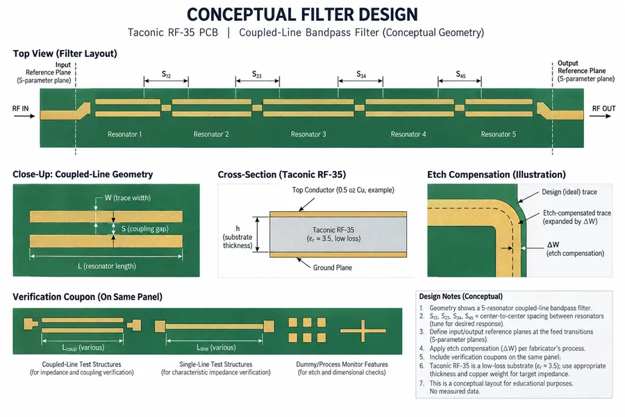
When the coupling gap, stackup, coupon, and inspection plan are released together, the team can tune the design deliberately. It can tell whether a response shift came from artwork, press construction, copper, finish, or the measurement fixture before changing the filter topology.
Project evidence and handoff for Taconic RF-35 PCB coupled line filter
For a coupled-line filter, preserve the original width, gap, length, mask condition, copper profile, dielectric target, tuning rule, and calibration plane. If a response moves, those fields allow the team to distinguish etch bias from an intentional tuning correction. The Taconic RF-35 PCB drawing should make the critical datum visible to layout, fabrication, assembly, and test. If a number is calculated, retain the assumptions; if it is a supplier typical, keep it labeled as typical; if it is a measured acceptance value, keep the sample, method, and revision traceable.
| Release item | Engineering question | Evidence to retain |
|---|---|---|
| Stackup and material | Does the finished construction match the RF model? | Finished dielectric target, copper assumption, material lot, cross-section |
| Transition or critical path | Is the mechanical datum also the electrical datum? | Launch drawing, via or pad dimensions, mask and connector inspection |
| Process witness | Does the coupon represent the product feature? | Panel position, layer pair, finish, drill and impedance record |
| Assembly and test | Could placement, rework, or calibration move the result? | Placement tolerance, reflow or rework history, fixture and reference plane |
For program control, use a short disposition statement after each build: what passed, what moved, what is still a target, and which owner decides the next change. This keeps the Taconic RF-35 PCB coupled line filter discussion focused on evidence and prevents a new material, finish, or layout change from being introduced without an updated model and acceptance plan.
Sources: Taconic and Rogers typical material data; IPC-TM-650 methods relevant to dielectric, copper, drilling, plating, registration, and impedance; RF application guidance from Qorvo, Analog Devices, and Würth Elektronik; KKPCB PCB design, materials, manufacturing, assembly, and high-frequency capability pages. Values are typical, target, or calculated references unless explicitly identified as measured.
