
Table of Contents
A Duroid 6010 PCB stackup is selected when a microwave project needs a controlled dielectric environment, compact routing, and repeatable transitions. The project risk is not solved by naming a laminate alone. It is solved when material documentation, finished dielectric, copper geometry, drilling, and coupon evidence all describe the same board. This guide gives engineers and project managers a practical path to a stable release without inventing customer measurements.
Why stackup control decides RF stability
Every Duroid 6010 PCB is a finished laminate-and-copper system. Press construction, copper foil, etch bias, plating, solder mask, and reference-plane continuity affect the field around each line and via. Supplier data is a starting reference; the released board still needs a controlled construction, drawing revision, and manufacturable process window.
A high-frequency PCB design review should distinguish typical material values, engineering targets, and measured coupon results. Freeze the material family, finished dielectric targets, copper weights, transition geometry, and impedance assumptions together. If a fabricator proposes another press construction, reopen the field review instead of silently scaling traces.
Seven controls for a reliable release
1. Freeze the finished dielectric
Record the post-lamination dielectric targets for every RF layer pair, including bondply and sequential steps. Use the finished construction—not the nominal catalog thickness—as the input to the field model. Add the material lot and stackup revision to the drawing and purchase package.
2. Tie trace geometry to copper profile
Show trace width, copper thickness, reference-plane distance, and etch compensation on the RF drawing. Copper profile and plating can move effective impedance, so the PCB manufacturing traveller should identify the intended compensation and cross-section location.
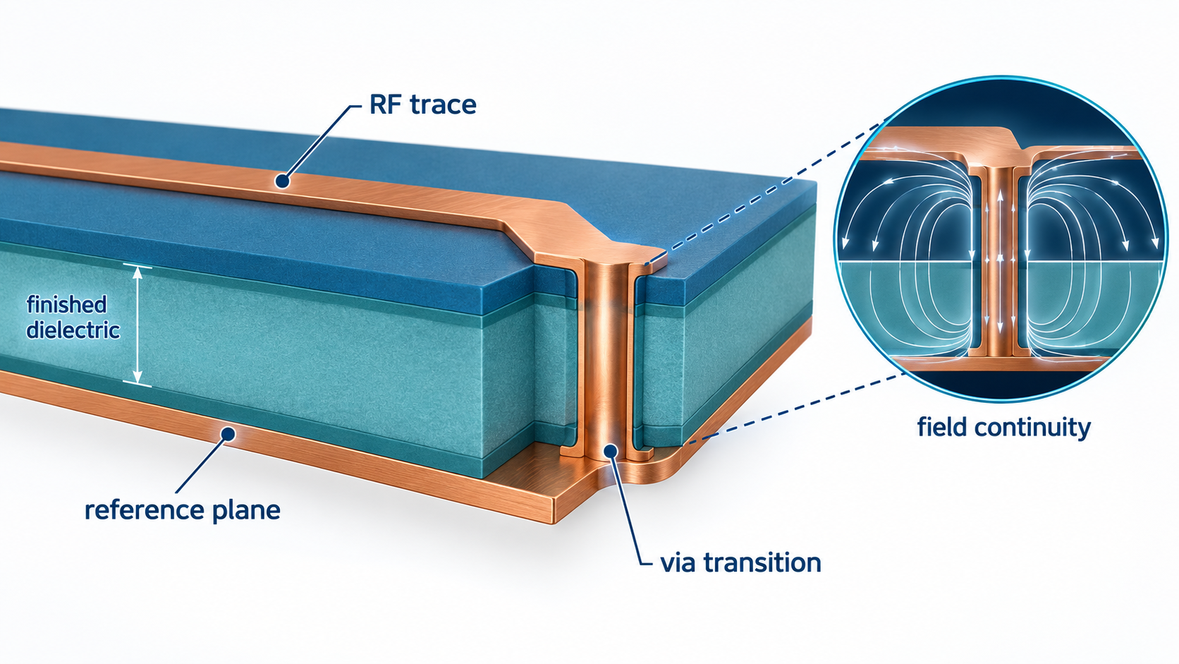
3. Plan transitions with return-current continuity
Review connector launches, vias, bends, and layer changes as complete structures. Keep reference planes continuous around the transition and place ground stitching where the field model requires it. A void or long via stub can dominate the result even when a straight trace meets its target.
4. Control drilling and plating
Specify finished hole, pad, antipad, annular ring, plating intent, and any back-drill feature. Tie drill registration and cross-section checks to the stackup revision. For a multilayer PCB build, identify sequential lamination and back-drill limits on the same release package.
5. Keep assembly datums aligned
Connector seating, solder fillets, fixtures, and board support can move an RF launch. The PCB assembly handoff should retain connector datums, mask openings, and the approved stackup revision. Label tuning pads as engineering options rather than measured performance claims.
6. Use a representative coupon
Choose coupon geometries that represent the critical microstrip, coplanar, via, or connector transition. Define coupon location, fixture, calibration, frequency range, and acceptance method before panel release. A coupon is process evidence for that revision, not a customer case study.
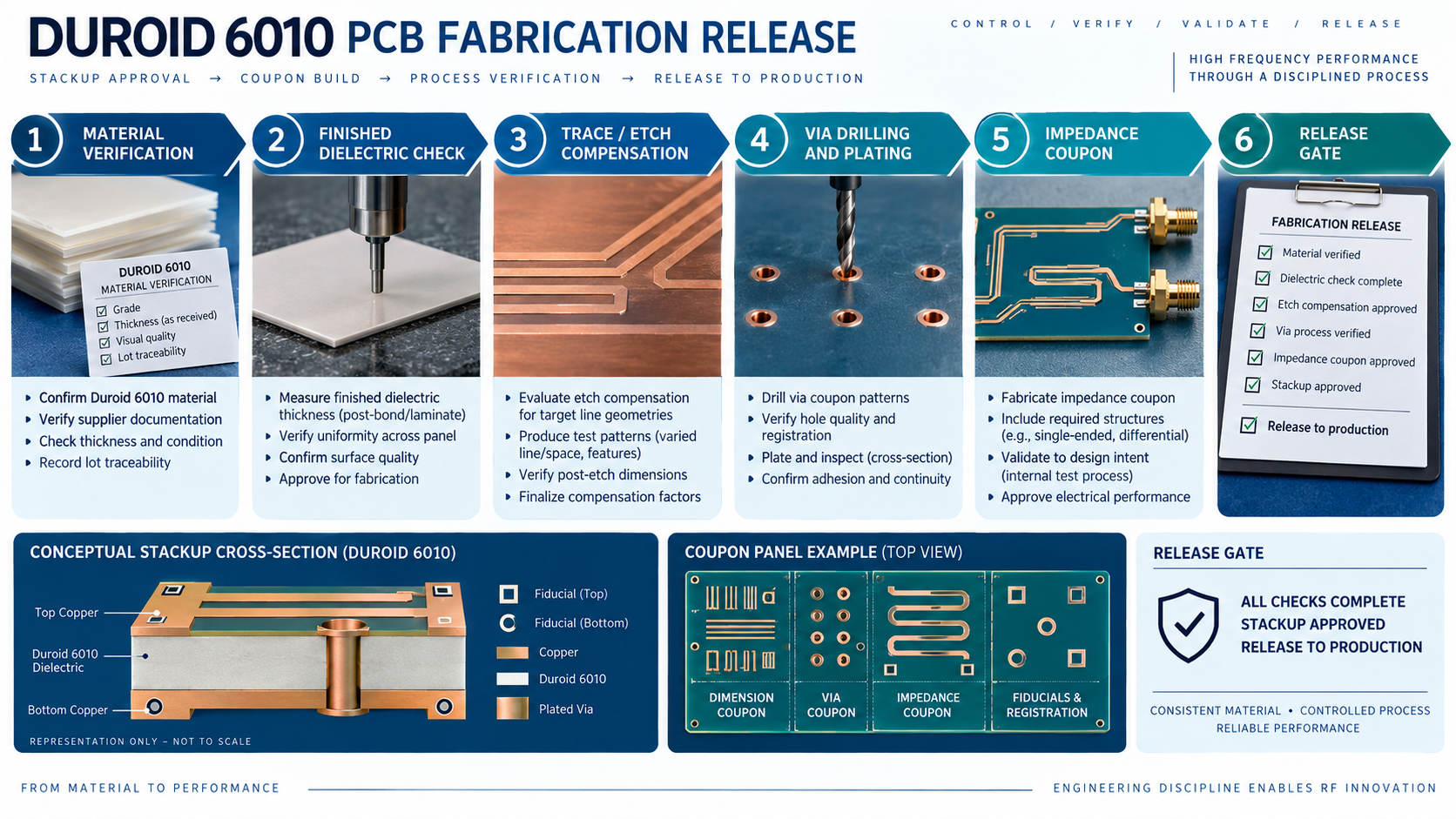
7. Carry traceability through release
Keep the material certificate, panel map, process revision, coupon location, and inspection disposition linked. The RF PCB manufacturing review should label typical, target, and measured values separately and identify which checks are required before shipment.
Project release checklist
- Finished dielectric, copper, drill, and impedance targets are revision controlled.
- Field-model assumptions match the approved cross-section and reference planes.
- Transition, ground-return, and back-drill features are visible on the fabrication drawing.
- Coupon geometry, fixture, calibration, and acceptance method are defined.
- Assembly datums and connector fixtures match the RF release package.
- Material lot and inspection disposition remain traceable to the build.
For procurement alignment, the Duroid 6010 PCB material page, the Duroid 6010 PCB fabrication page, and the Duroid 6010 PCB RF capability page should point to the approved construction. The goal is a Duroid 6010 PCB package in which design, fabrication, coupon, and assembly teams make decisions from one controlled revision.
Sources: Rogers Corporation RT/duroid 6010 material information and fabrication guidance; IPC-TM-650 methods for dielectric, drilling, plating, registration, and impedance-related checks; KKPCB internal high-frequency DFM capability notes. Values are typical or target references unless explicitly identified as measured.
