
Contents
Duroid 5880 PCB stackup decisions determine whether an RF design can move from field model to repeatable fabrication. A nominal dielectric value is not enough. Pressed thickness, copper foil, roughness, trace geometry, and coupon correlation all influence the finished transition. This article gives project teams a practical stackup-release method without presenting unverified customer measurements.
Why stackup drift changes RF behavior
A Duroid 5880 PCB is a built structure, not a single material sheet. PTFE layers, copper foils, plated holes, mask, and mechanical compression interact during lamination and imaging. A change in finished dielectric or copper profile changes the field distribution even when the artwork file is unchanged.
Freeze the approved Duroid 5880 PCB stackup, material lot, copper weights, and impedance targets in one revision. A high-frequency PCB design review should show which dimensions are targets, which are typical material values, and which will be verified on a coupon.
Six stackup and impedance controls
1. Define the finished dielectric target
Record the finished dielectric thickness after press, not only the nominal core thickness. Note the press construction, bondply, copper foil, and any sequential-lamination step. Every Duroid 5880 PCB release should identify the stackup revision used by the field model.
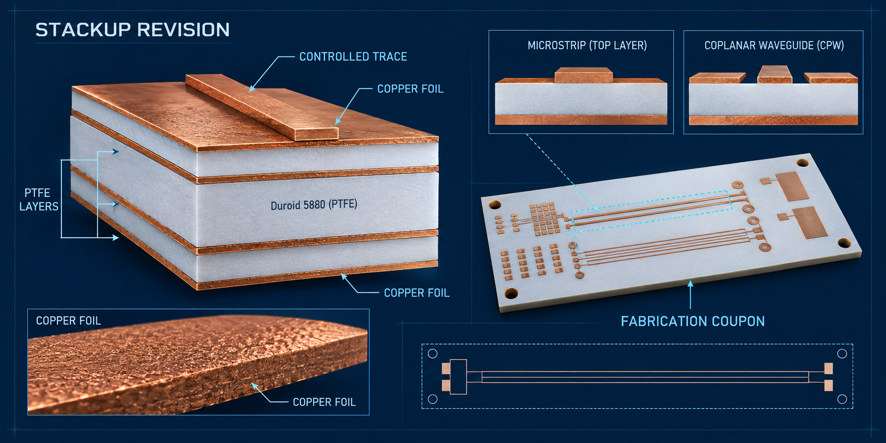
Conceptual PTFE stackup, controlled trace, copper foil, and fabrication coupon.
2. Keep the field model tied to the stackup
A second Duroid 5880 PCB stackup revision must trigger a field-model comparison.
Use the approved trace width, copper thickness, reference-plane distance, and dielectric target in the model. If the fabricator proposes a different press construction, compare the electromagnetic assumptions before approving the substitution. The PCB materials record should show the manufacturer data used as the starting point.
3. Treat copper profile as an RF variable
The Duroid 5880 PCB fabrication traveler should identify the copper and etch assumptions.
Copper roughness and foil profile influence loss and effective impedance. Do not hide the assumption in a spreadsheet. State it on the stackup drawing and flag the tolerance that needs process control. A PCB manufacturing review can align foil, etch compensation, plating, and cross-section checks.
4. Separate target, typical, and measured values
Material datasheets provide typical values. Engineering targets belong to the approved drawing. Measured values belong to a traceable coupon, fixture, calibration, and lot. For a Duroid 5880 PCB, keeping these labels separate prevents a nominal value from being misread as a qualification result.
5. Design a representative coupon
Place coupon traces that represent the critical microstrip, coplanar, via, or connector transition. Define coupon location, panel position, calibration method, and frequency range before production. The coupon should be tied to the same stackup revision as the Duroid 5880 PCB panel.
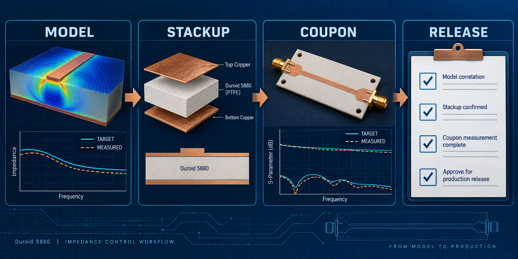
Conceptual model-to-stackup-to-coupon workflow with target and measured labels.
6. Close the release with DFM and assembly
For a Duroid 5880 PCB build, keep the approved stackup with the assembly and back-drill record.
Check drill, annular ring, layer registration, solder mask, connector launch, and panel balance before releasing the stackup. A PCB assembly review should confirm that component pads, connector seating, and fixture datums match the RF geometry. For a multilayer PCB build, also identify sequential-lamination and back-drill features.
Coupon and release workflow
Move from MODEL to STACKUP to COUPON to RELEASE. First, document the field assumptions. Second, approve the pressed construction and copper. Third, fabricate a representative coupon with the panel. Finally, compare the evidence to the agreed acceptance method. A process coupon is evidence for its revision, not a customer case study.
For each Duroid 5880 PCB lot, retain the stackup drawing, material certificate, panel map, coupon location, inspection record, and engineering disposition. If the lot is split or a press cycle changes, reopen the review instead of copying the previous approval.
Duroid 5880 PCB stackup release checklist
- Finished dielectric targets and press construction are revision controlled.
- Field-model assumptions match trace, copper, and reference-plane dimensions.
- Typical material values, engineering targets, and measured values are labeled.
- Coupon geometry represents the critical RF transitions.
- Drill, plating, registration, mask, and panel DFM limits are manufacturable.
- Assembly fixtures and connector datums match the RF drawing.
The approved Duroid 5880 PCB stackup should remain the single source for design, fabrication, coupon, and assembly decisions. KKPCB can review the stackup package, impedance targets, coupon plan, and manufacturing handoff as one controlled release.
Sources: Rogers Corporation RT/duroid 5880 material information and fabrication guidance; IPC-TM-650 methods for dielectric, drilling, plating, registration, and impedance-related process checks; KKPCB internal high-frequency DFM capability notes. Values are typical or target references unless explicitly identified as measured.
