
Microwave design teams often choose Duroid 5880 for its low-loss behavior, then discover that stackup translation and fabrication details decide whether the finished board matches the model. A production-ready Duroid 5880 PCB needs a controlled dielectric reference, consistent copper geometry, and inspection points that survive panel processing. This guide turns those requirements into a practical release workflow for RF engineers, layout teams, and project managers.
Contents
Start with a stackup model the factory can build
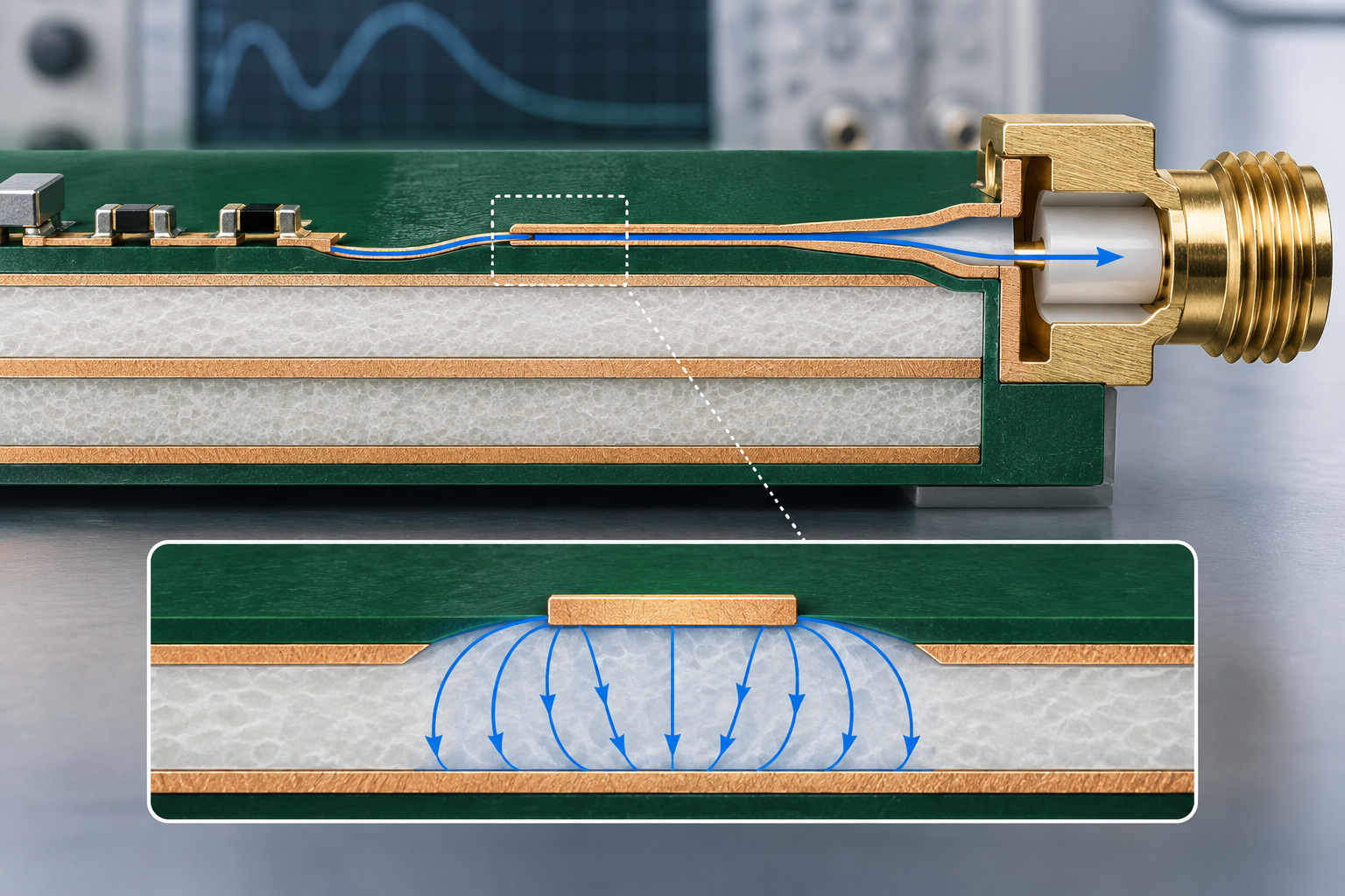
The stackup should identify layer order, finished copper, dielectric references, prepreg or bonding film, and the intended impedance geometry. When a design includes mixed materials or a metal carrier, show where the Duroid section begins and ends. A controlled-impedance PCB review should compare the modeled trace to the finished cross-section rather than copying a nominal catalog thickness into the drawing.
Rogers publishes typical RT/duroid 5880 properties and processing guidance. Those values help establish a model, but they are not a build-specific guarantee. Mark typical material values, engineering targets, and measured results separately. This keeps the Duroid 5880 PCB release technically honest when material construction or copper roughness changes.
Protect the RF field during layout translation
Keep reference planes continuous
A low-loss laminate cannot compensate for a broken return path. Keep the reference plane continuous under feeds, bends, and connector launches. If a plane slot is necessary for mechanical clearance, document the transition and review the effect on the field. The drawing should also identify antenna keep-outs, via fences, and the plane used for impedance control.
Separate RF geometry from manufacturing fill
Copper fill helps imaging and lamination, but it must stay outside sensitive lines and apertures. A high-frequency PCB review should show the RF exclusion zones and approved balance regions together. Do not allow a late panel-fill edit to move a trace edge or change the local reference-plane distance.
Control drilling, plating, and registration
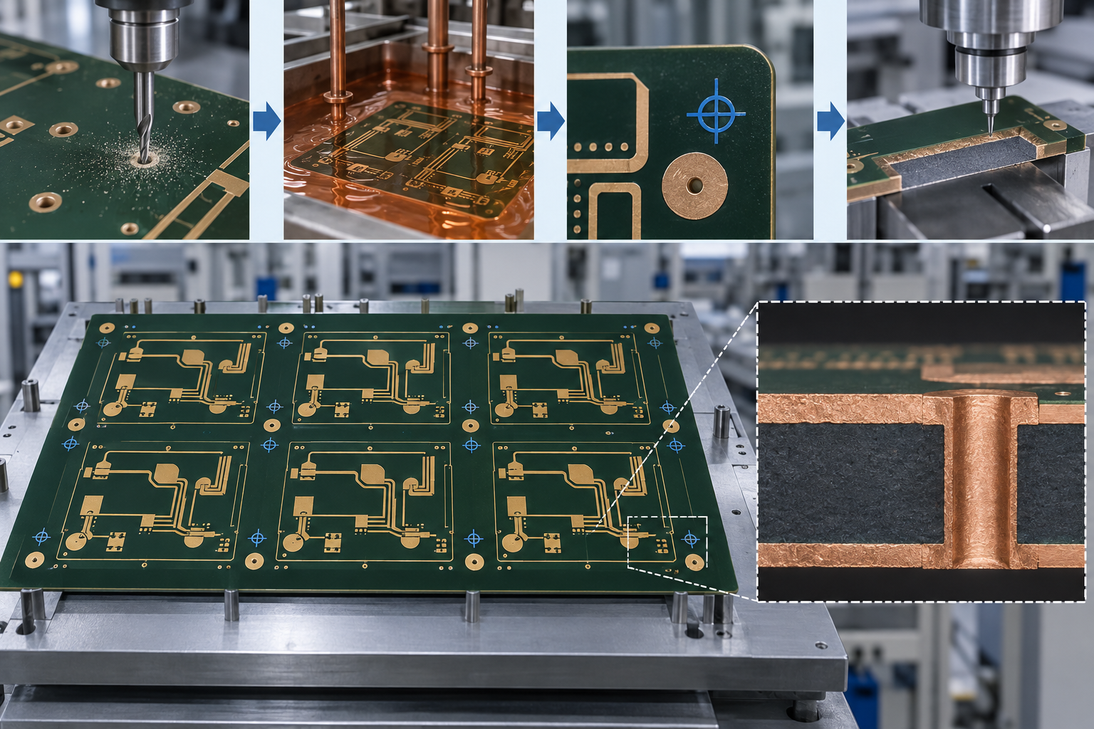
Duroid constructions can be damaged by aggressive drilling or unsupported handling. Define drill entry, tool selection, smear control, desmear, plating, and inspection requirements in the fabrication notes. For plated RF vias, review finished hole, capture-pad geometry, aspect ratio, and the relationship to adjacent ground vias. If a sequential or hybrid build is used, identify the registration datum for every lamination cycle.
Registration should be reviewed from the individual board through the panel. Tie tooling holes, fiducials, connector launches, and antenna references to one master datum. The PCB manufacturing handoff should state which dimensions are targets and which require measurement. This prevents a drawing tolerance from being mistaken for an actual process capability.
Use panel and coupon evidence
A witness coupon can confirm layer order, plated-via continuity, finished thickness, and registration. Place coupons where copper density and panel position make them representative. If the project needs electrical correlation, define the coupon geometry, fixture, frequency range, calibration, and acceptance rule before release. A coupon is process evidence; it is not a customer measurement or a substitute for product qualification.
Record panel ID, material construction, lot, drill program, lamination revision, surface finish, and inspection disposition. When a feature shifts between center and edge positions, review panel balance and registration before changing the RF layout. This traceability helps the RF PCB assembly team separate fabrication variation from placement or connector seating effects.
Duroid 5880 PCB release checklist
- Define a buildable stackup with layer order, finished copper, and dielectric references.
- Protect continuous reference planes, RF keep-outs, and via-fence returns.
- Freeze drill, desmear, plating, and registration requirements.
- Separate typical material data, design targets, and measured evidence.
- Place representative coupons and trace their panel position and lot.
- Document surface finish, connector interface, and assembly datum.
- Review every panel-fill or stackup revision against the RF model.
KKPCB can review a multilayer Duroid 5880 PCB package for stackup, registration, drilling, plating, coupon design, and assembly handoff. The objective is a drawing that exposes process risk while revisions are still inexpensive.
Key takeaway
A reliable Duroid 5880 PCB is created by aligning the RF model with a buildable stackup, protected return path, controlled fabrication process, and traceable evidence plan. Keep material references distinct from measured results, keep RF geometry visible through panelization, and make every changed variable part of the release review.
Sources: Rogers Corporation RT/duroid 5880 material information and fabrication guidance; IPC-TM-650 methods for printed-board drilling, registration, and cross-section inspection; KKPCB internal high-frequency DFM capability notes. Values are typical or target references unless explicitly identified as measured.
