At microwave frequencies, the connector launch is often the first place where a good laminate stackup loses repeatability. The RO5880 PCB release should therefore treat the launch as a controlled subassembly. The finished RO5880 PCB must hold the launch geometry, surface finish, and reference-plane relationship while it moves through panel fabrication and assembly. This guide gives RF engineers and project managers a practical release method for avoiding launch mismatch, pad damage, and inspection gaps without claiming unverified customer results.
Why the connector launch deserves its own control plan
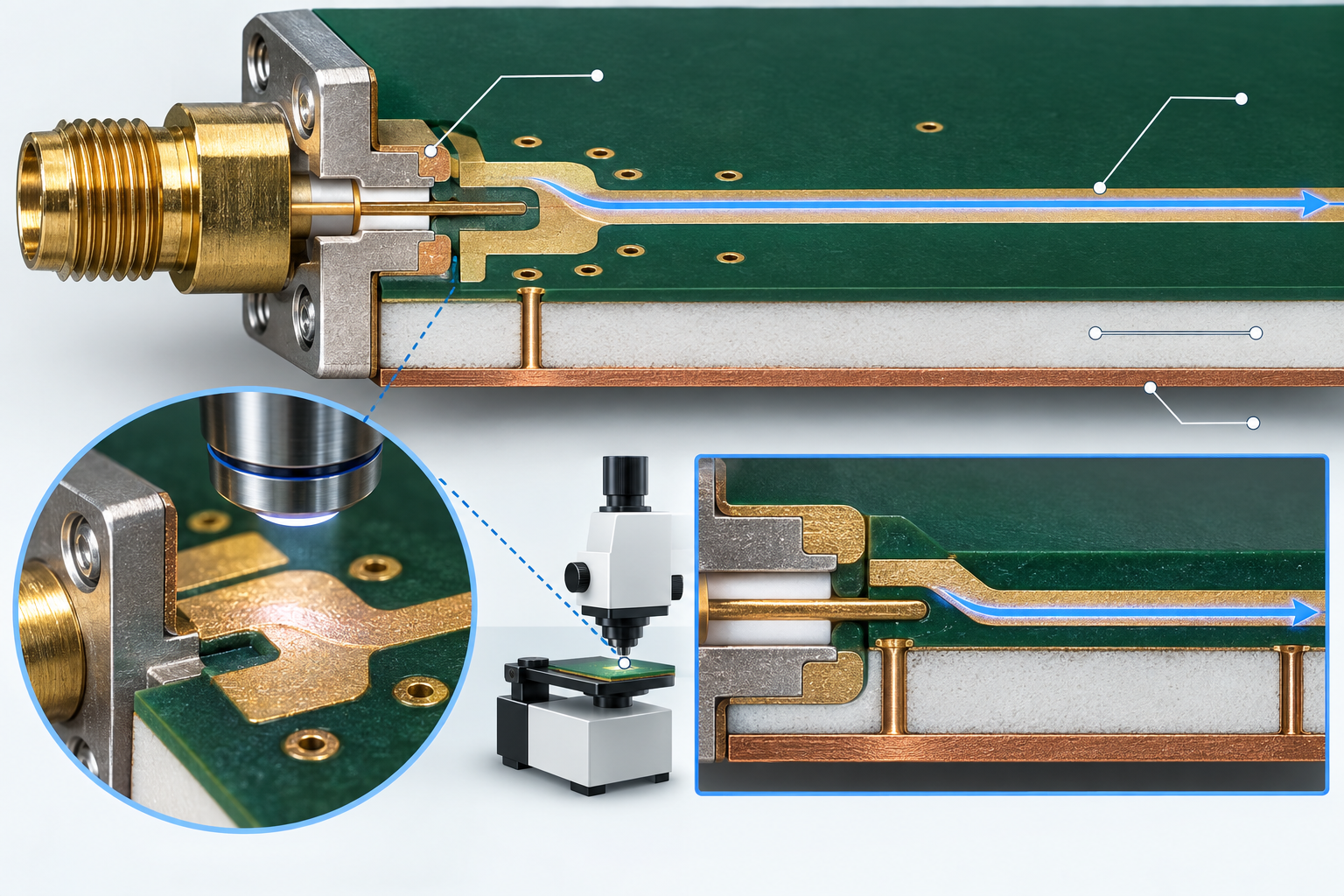
A coaxial launch is a short transition between a connector pin, plated pad, dielectric, and return path. Small changes in pad length, mask clearance, or ground-via position can change the local field before the signal reaches the routed line. Treat the launch as a controlled structure in the RF connector launch drawing, with a single datum shared by fabrication, assembly, and test.
On an RO5880 PCB, the laminate’s low-loss behavior does not automatically make the connector transition repeatable. The drawing should identify the finished copper surface, plating callout, solder-mask keep-out, reference-plane opening, and nearby via fence. This keeps the RO5880 PCB launch definition stable when the connector footprint is revised. Each item must be reviewed against the connector supplier’s mechanical envelope and the approved stackup.
Conceptual RO5880 PCB connector launch showing the RF path, reference plane, and inspection view.
Lock launch geometry before choosing the finish
Use the connector datum as the electrical datum
Place the connector mounting holes, signal pad, ground pads, and first transition vias from one mechanical origin. If the launch is copied across a panel, preserve the same rotation and mirror rules. A controlled-impedance PCB review should compare the launch cross-section with the routed line, not only the nominal footprint. This prevents a footprint update from silently changing the reference-plane distance.
Keep mask and plating decisions visible
Define whether the signal pad is mask-defined or copper-defined, then show the clearance on the fabrication drawing. The approved surface finish must be named on the same drawing. Surface finish must be selected for the connector contact, soldering method, and RF loss budget. A finish that is acceptable for a general board may create a different pad edge, roughness, or solder wetting behavior at a microwave launch. Record the finish as a process requirement, not as a note hidden in a purchasing file.
Coordinate RF launch details with assembly
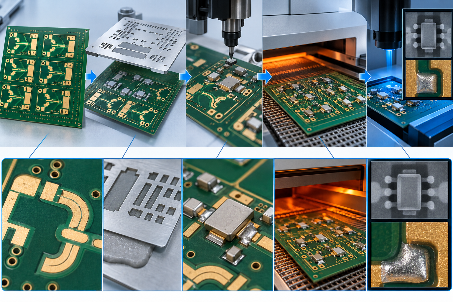
The assembly line sees the launch as a placement and solder-joint problem. Paste apertures, component keep-outs, connector seating, and reflow support can all move the electrical transition. For a mixed RF and digital panel, separate connector pads from high-volume SMT apertures so stencil changes do not alter the launch by accident. The SMT assembly traveler should identify connector orientation, torque or seating instructions when applicable, and the inspection view required after reflow.
Use a small witness region on the panel to check paste release, pad condition, and solder wetting. That witness is not a customer test result; it is a process monitor that lets the team compare a new stencil, finish lot, or reflow recipe against the approved baseline. Keep the witness location and revision with the panel ID.
Conceptual RF assembly flow with stencil, placement, reflow, and post-assembly inspection.
Build an inspection plan that follows the RF path
Visual inspection should confirm pad shape, mask clearance, connector seating, and solder fillet condition. For every RO5880 PCB lot, record the launch revision before inspection. Cross-section coupons can verify layer order, plated interconnects, and the relationship between the launch pad and reference plane. If a project requires electrical correlation, define the fixture, frequency range, calibration method, and acceptance rule before the first panel is built. Do not replace that method with a generic statement that the RO5880 PCB manufacturing route is “RF qualified.”
Record panel position, material construction, surface-finish lot, stencil revision, reflow profile revision, and inspection disposition for the RO5880 PCB. If a return-loss shift appears later, this traceability lets the team separate connector seating from laminate, plating, or assembly causes. The evidence should distinguish typical material behavior, engineering targets, and measured values. This record gives the RO5880 PCB team a clear baseline for the next revision.
RO5880 PCB connector-launch release checklist
Share one datum across connector, RF layout, tooling, and inspection.
Show pad definition, mask clearance, finish, and reference-plane opening.
Review the launch cross-section against the routed controlled-impedance line.
Freeze stencil, seating, reflow, and inspection instructions for the RF connector.
Place a witness coupon or witness region where it can expose process drift.
Trace panel position, material lot, finish lot, and process revisions.
KKPCB can review a RO5880 PCB launch package, including stackup, connector footprint, surface finish, and witness design, before releasing a multilayer panel. The review goal is to make the RF transition inspectable and repeatable rather than relying on a nominal footprint.
Key takeaway
A reliable launch is a coordinated mechanical, electrical, and assembly structure. When the datum, finish, mask, plating, and inspection method are locked together, an RO5880 PCB can move from prototype to volume production with fewer surprises. Use the process record to explain any measured change, and keep design targets separate from typical laminate data. That discipline gives each RO5880 PCB revision a traceable engineering decision.
Sources: Rogers Corporation RT/duroid 5880 material information and fabrication guidance; IPC-TM-650 methods for printed-board inspection and dimensional control; KKPCB internal high-frequency DFM capability notes. Values are typical or target references unless explicitly identified as measured.