
At millimeter-wave frequencies, a small dielectric or registration change can move the phase of an antenna feed enough to reduce array margin. The practical question is not simply whether an RO4835 PCB is low loss; it is how the stackup, copper geometry, and fabrication handoff keep phase repeatable from prototype to production. This engineering guide presents an illustrative 77 GHz feed-network decision and clearly separates vendor-typical values from design targets. The selected PCB materials and finished dimensions must remain traceable through release.
Translate material variation into a phase budget
Rogers publishes RO4835 typical process Dk around 3.48 ± 0.05 at 10 GHz, with a design Dk of 3.66 for the standard laminate family. The RO4835IND LoPro data sheet gives a different design context for automotive radar, including design Dk around 3.48 at 60 GHz and 3.49 at 77 GHz. These values must not be mixed: the correct laminate variant, frequency range, copper treatment, and supplier construction belong in the project stackup file. For an RO4835 PCB, the design Dk must stay tied to the operating band.
| Phase-risk source | Why it matters | Engineering response |
|---|---|---|
| Dk model mismatch | Phase length calculated with a generic FR-4 or the wrong Rogers test value. | Use the selected variant’s design Dk and document the frequency assumption. |
| Dielectric thickness | Press variation changes effective permittivity and trace impedance. | Specify finished dielectric and recalculate the phase delay for the released build. |
| Copper roughness | Loss and effective propagation change as the conductor profile changes. | Call out copper treatment and preserve it through prototype and volume tooling. |
| Layer registration | Feed and via centers shift relative to the antenna or connector. | Use registration targets and a DFM review for every RF transition. |
Choose a stackup for repeatable RF geometry
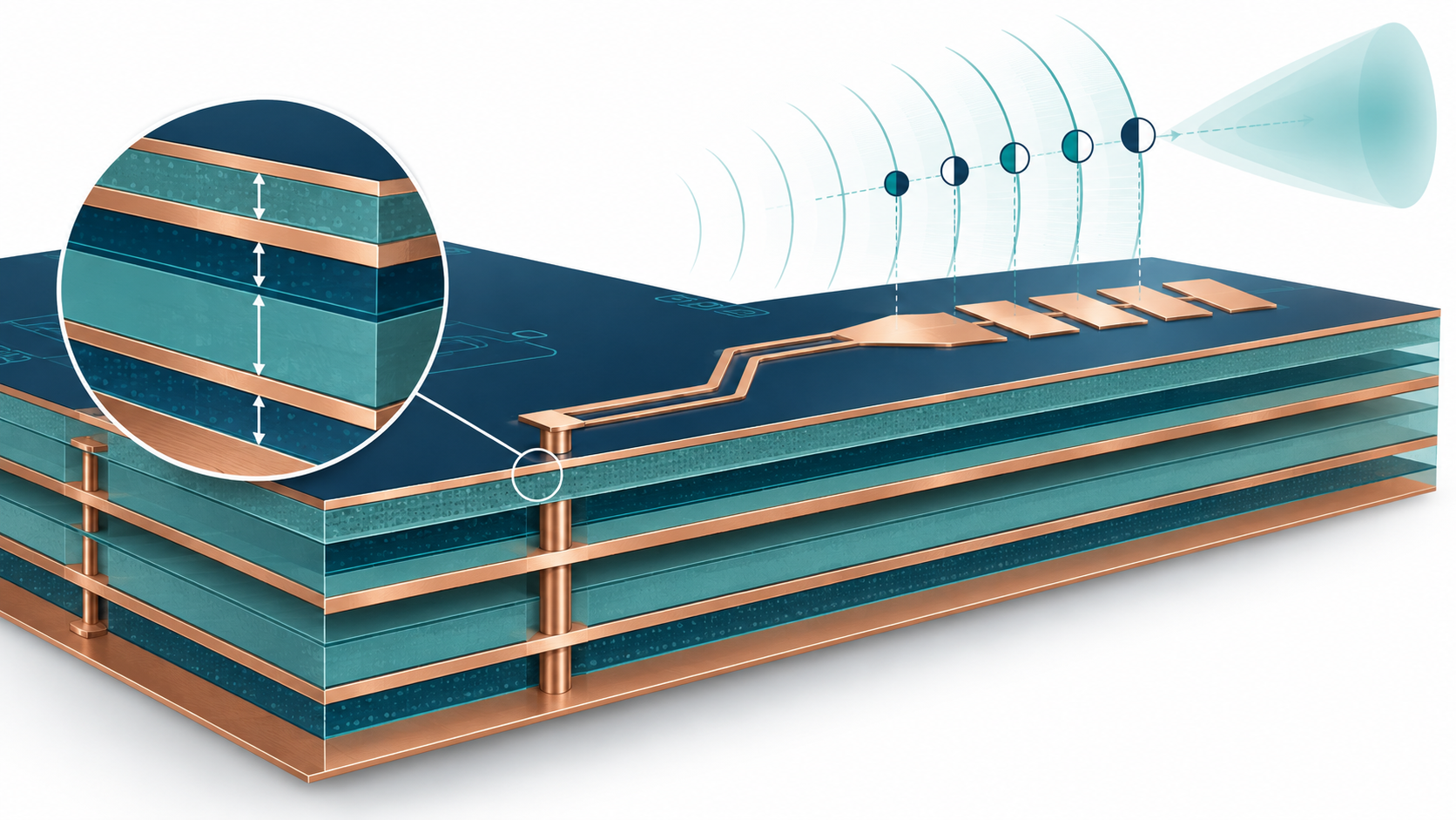
A robust RO4835 PCB stackup keeps the antenna feed close to a continuous reference plane and avoids unnecessary material interfaces under the controlled line. For a compact module, a hybrid construction can place RO4835 near the RF feed while using standard cores for digital routing. The hybrid boundary must be modeled because resin distribution, plane spacing, and via transitions can change the effective line environment. The resulting high-frequency PCB geometry belongs in the same controlled stackup record.
For a 77 GHz illustrative design target, the team might reserve one thin controlled-dielectric layer for the feed, use adjacent solid planes, and route bias lines on a shielded layer. This RO4835 PCB decision should be treated as a phase-control problem, not a material-name lookup. The target is not a claimed KKPCB measurement. It is a planning example that must be re-solved with the selected finished thickness and copper profile before fabrication.
Keep phase-critical dimensions explicit
Do not bury phase-critical geometry in a generic impedance note. Identify the feed length, bend radius, launch pad, via antipad, solder-mask opening, and antenna reference edge. When a build uses an HDI PCB escape, specify whether the microvia is stacked or staggered and how the pad and capture geometry are referenced to the RF plane.
Control transitions and return current at 77 GHz
The feed transition is often the first place where a nominally correct stackup loses phase margin. Keep the launch short, make the ground transition symmetric, and avoid a plane void that forces return current around a connector or via field. A short design review that overlays the RF path, reference planes, and mechanical keep-outs is usually more valuable than adding another decimal place to the material Dk.
For a production RO4835 PCB release, the fabricator should receive the laminate variant, finished dielectric targets, copper treatment, surface finish, registration tolerance, and coupon definition. If any item changes, the team should update the phase and impedance model before approving the first article.
Illustrative project case: preventing array beam skew
Imagine an automotive radar feed network in which a prototype meets the simulated beam angle but a second panel shows a small array skew. This is an illustrative failure mode, not a KKPCB customer case. The investigation should compare three records: the released stackup, the pressed cross-section, and the RF coupon or transition result. If the laminate variant changed from standard RO4835 to a LoPro option, the Dk model and loss assumptions must be updated rather than treating the materials as interchangeable.
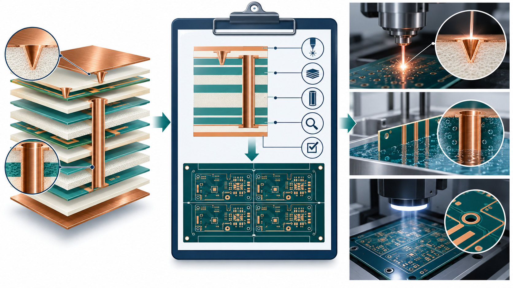
A disciplined PCB manufacturing handoff for the RO4835 PCB also records panel position, copper balance, lamination direction, drill registration, and the inspection points for feed and antenna features. KKPCB’s public manufacturing information describes high-frequency, multilayer PCB, mixed-material, sequential-lamination, and HDI services, while the exact process window remains quotation-specific.
Validation plan without overclaiming measurements
- Lock the selected RO4835 variant and its frequency-appropriate design Dk source.
- Run a field-solver calculation using the released finished dielectric and copper profile.
- Check the feed and transition against the same plane geometry used in the model.
- Inspect first-article cross-section and registration against the drawing.
- Measure the approved coupon or RF transition and label the result as measured only when recorded by the project quality system. Keep the RO4835 PCB acceptance record with the released build.
Release checklist for project managers
- One exact material variant is named; the released RO4835 PCB stackup carries no implicit equivalent substitution.
- Dk, Df, thickness, and copper data are tagged as vendor-typical or design target.
- Phase-critical dimensions and RF transitions are visible in the fabrication package.
- Hybrid boundaries and HDI microvia structures are included in the DFM review.
- Prototype and production builds use the same coupon and acceptance logic.
Project questions to resolve before release
Which RO4835 PCB variant is in the model?
Confirm the exact RO4835 PCB variant, operating band, finished dielectric, and copper treatment before the solver or drawing is released. A material family name alone is not enough for a phase-critical radar feed.
What changes when the build changes?
If an RO4835 PCB build changes thickness, resin system, copper profile, or registration class, update the impedance and phase model and repeat the agreed coupon review. Do not carry a previous acceptance result forward by assumption.
How should first article acceptance be recorded?
The RO4835 PCB first-article record should tie the cross-section, registration inspection, transition coupon, and drawing revision to one lot. This makes a later production comparison auditable without implying an unverified customer measurement.
Sources: Rogers RO4835 and RO4835IND LoPro manufacturer data are used as vendor-typical reference values; KKPCB public PCB materials, RO4835 detail, high-frequency PCB, HDI PCB, and PCB manufacturing pages are used to verify service categories. This article contains no external hyperlinks and does not claim a KKPCB customer measurement.
