
Engineering intent. A phased array can lose beam accuracy when equal-looking traces have different electrical lengths or transitions. This article explains how to plan an RO3003 PCB feed network for a conceptual phased-array module. It separates layout targets from measured production data and does not claim a KKPCB customer case study.
RO3003 belongs to the Rogers RO3000 family of ceramic-filled PTFE laminates. Use the supplier data under its stated test method, then replace assumptions with the finished dielectric, copper, connector, and enclosure values that apply to the released board.
Define the array before drawing the feed tree
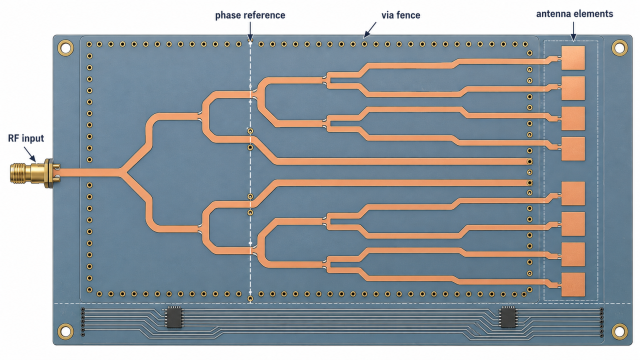
Start with element count, operating band, polarization, scan range, transceiver location, and the required amplitude and phase balance. A feed network is not just a set of equal-length lines; it includes the splitter topology, reference plane, layer changes, bends, pads, and antenna launch.
For a fabrication-ready RO3003 PCB, put the array boundary, transceiver boundary, and connector datum on the same planning drawing. Keep digital clocks, switching converters, and high-current returns outside the active aperture whenever the enclosure allows.
Choose a feed topology that can be reviewed
Corporate and series-fed options
A corporate feed offers explicit split points and can make amplitude and phase rules easier to document. A series-fed arrangement may reduce routing area but couples the behavior of one element to the next. Record why the topology was selected instead of treating a generic reference design as a universal answer.
| Feed decision | Question to answer | Layout evidence |
|---|---|---|
| Splitter order | Are branch impedances and phase references defined at every split? | Annotated feed tree and stackup reference. |
| Line form | Does each branch use microstrip or grounded coplanar waveguide consistently? | Cross-section and width-gap rules. |
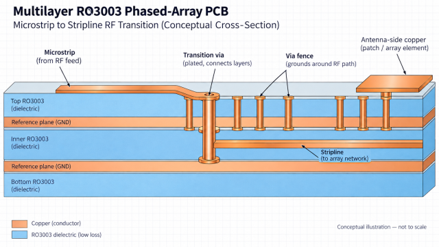
| Layer changes | Where are signal vias, ground vias, and stubs controlled? | Transition drawing with antipad notes. |
| Array launch | How does the feed connect to the radiator or package? | Launch footprint and enclosure datum. |
The PCB layout review should compare the feed tree with the approved phase model before detailed routing begins.
Match electrical length, not only geometry
Two traces can have the same centerline length but different phase delay if they use different dielectric spacing, copper profiles, bends, or transitions. Keep branches on the same layer and line form when practical. If a layer change is required, include the signal via, antipad, nearby ground vias, and any residual stub in the model.
Use a branch table that records target electrical length, nominal physical length, reference plane, and allowed tolerance. The target is a design requirement; it is not evidence that a finished board has achieved the value.
At each splitter, preserve a continuous return path and avoid plane slots underneath the junction. A high-frequency PCB capability review should verify that the proposed via fence, registration budget, and copper treatment can be built as drawn.
Control coupling and via-fence behavior
Ground boundaries
Via fences can contain fields and provide a nearby return path, but their pitch, drill size, and distance from the trace are stackup-dependent. Avoid copying a fence rule from another laminate without checking the finished construction.
Parallel branches
Keep parallel feed branches separated where coupling would change amplitude or phase. If a crossover is unavoidable, use a validated transition and document the reference planes on both sides. The board-level result also depends on the radome, package, and mechanical cover.
Record the assumptions in the PCB materials selection and fabrication note. Do not present a simulated S-parameter curve or measured beam plot unless it is backed by an identified source.
Build a verification plan for the first prototype
A useful verification plan connects the feed network to fixtures and system requirements. Define the calibration plane, connector, test coupon, and acceptance limits before the board is built. Then compare return loss, insertion loss, phase balance, and beam behavior with the design targets.
| Gate | Evidence | Release decision |
|---|---|---|
| Architecture | Array geometry, feed topology, and phase targets | Approve the network concept. |
| Layout | Electrical lengths, return paths, and via fences | Approve the routed geometry. |
| Fabrication | Finished dielectric, copper, drilling, and registration notes | Release the build package. |
| Prototype | Fixture-based RF measurements at defined conditions | Compare with targets and record deviations. |
KKPCB can review the PCB manufacturing services requirements for controlled features, drilling, lamination, and inspection. The review preserves design intent; it does not guarantee a particular array pattern.
For the design record, map the measured or modelled transitions back to the RO3003 PCB stackup and identify the exact condition of every comparison.
Release checklist for a phased-array feed
- Freeze array geometry, splitter topology, and the transceiver datum.
- Use a single reference construction for matched branches where possible.
- Document electrical length and tolerance, not only drawn length.
- Review via fences, antipads, plane voids, and connector launches together.
- Separate supplier typical values, model targets, and measured prototype results.
Before changing a layer or connector, verify that the RO3003 PCB phase table and the released drawing remain aligned.
If fabrication changes the press construction or drilling method, update the RO3003 PCB build notes and repeat the affected model checks.
Sources: Rogers RO3000 Series Laminates product information; Rogers RO3000 laminate data sheet for RO3003; Rogers fabrication guidelines for RO3000 and RO3200 series high-frequency circuit materials. Supplier values are used under their stated conditions and are not finished-board measurements.
For RF module sourcing, review KKPCB’s RF PCB manufacturing route before locking the feed topology.
