What is an HDI PCB?
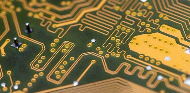
An HDI PCB (High-Density Interconnect PCB) is an advanced printed circuit board designed with higher wiring density per unit area, using technologies such as microvias, fine lines, and sequential lamination.
Compared to conventional PCBs, an HDI PCB enables more compact layouts, improved electrical performance, and higher signal density, making it essential for modern electronic devices.
Typical HDI PCB features include:
- Microvias (laser-drilled vias)
- Fine line and spacing
- Multiple build-up layers
- High layer count with compact size
Why HDI PCB Technology Matters
As electronic products become smaller and more powerful, standard PCB technology reaches its limits. HDI PCB technology allows:
- Increased routing density in limited space
- Reduced signal path length
- Improved signal integrity
- Better electrical performance for high-speed designs
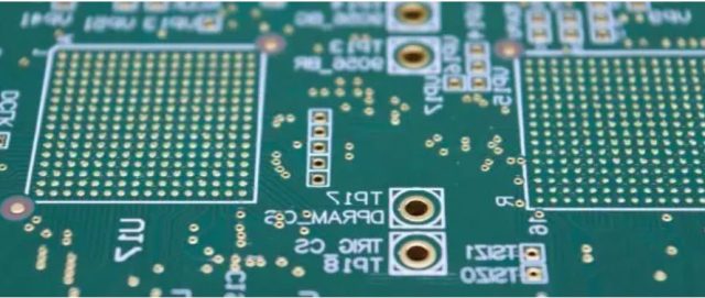
Key Features of HDI PCB
1. Microvia Technology
Microvias are a defining feature of HDI PCB, enabling vertical interconnections between layers with minimal space.
2. Fine Line Circuitry
HDI PCB supports ultra-fine trace width and spacing, allowing higher circuit density.
3. Sequential Lamination
Multiple lamination cycles are used to build complex HDI PCB stack-ups.
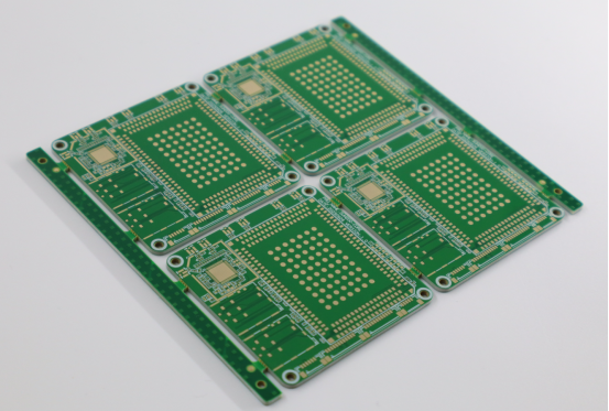
4. High Layer Density
HDI PCB designs can achieve more functionality within fewer layers compared to traditional PCBs.
Common HDI PCB Stack-Up Structures
1. 1+N+1 Structure
- One build-up layer on each side
- Entry-level HDI PCB
2. 2+N+2 Structure
- Two build-up layers per side
- Higher routing density
3. Any-Layer HDI PCB
- Microvias between any layers
- Maximum design flexibility
HDI PCB vs Standard PCB
| Feature | HDI PCB | Standard PCB |
|---|---|---|
| Wiring Density | High | Moderate |
| Via Type | Microvia | Through-hole |
| Size | Compact | Larger |
| Performance | High-speed capable | Limited |
| Cost | Higher | Lower |
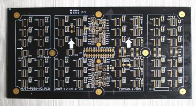
Applications of HDI PCB
1. Smartphones & Tablets
HDI PCB enables compact layouts and high integration.
2. Wearable Devices
Space-saving design requires HDI PCB technology.
3. High-Speed Computing
Servers and processors benefit from HDI PCB signal performance.
4. Automotive Electronics
ADAS and control systems use HDI PCB for reliability and compactness.
5. Medical Devices
Miniaturized and high-precision HDI PCB designs are essential.
Manufacturing Challenges of HDI PCB
Producing a high-quality HDI PCB requires advanced capabilities:
1. Laser Drilling Precision
Microvias must be accurately formed without damaging surrounding material.
2. Registration Accuracy
Layer alignment is critical for HDI PCB performance.
3. Sequential Lamination Control
Multiple lamination cycles increase complexity and risk.
4. Yield Management
Higher density increases the probability of defects.
Design Considerations for HDI PCB
1. Optimize Stack-Up Early
HDI PCB performance depends heavily on stack-up design.
2. Control Via Structure
Avoid unnecessary via stacking to reduce risk.
3. Balance Density and Manufacturability
Overly aggressive design reduces yield.
4. Collaborate with Manufacturer
DFM is critical in HDI PCB projects.
When Should You Use HDI PCB?
Choose HDI PCB when:
- Product size is highly constrained
- High pin-count components are used
- High-speed signal routing is required
- Design complexity exceeds standard PCB capability
Avoid HDI PCB when:
- Cost is the primary concern
- Design density is low
- Standard PCB can meet requirements
Conclusion
HDI PCB technology is a core enabler of modern electronics, supporting compact, high-performance, and high-density designs.
With the right design approach and manufacturing expertise, HDI PCB delivers superior electrical performance, space efficiency, and reliability.
