What Makes an ATE PCB Truly “Custom”?
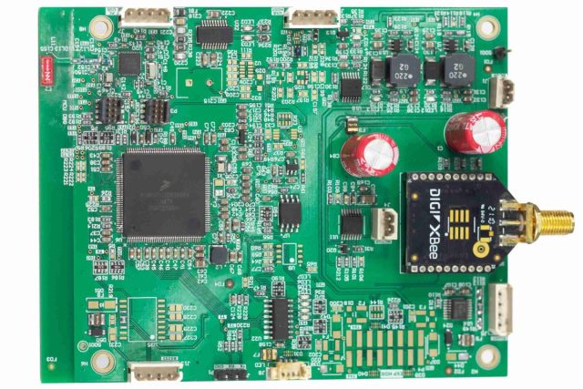
A Custom ATE PCB is not just a modified test board—it is a fully tailored interface designed around a specific combination of:
- Device Under Test (DUT)
- Test socket and mechanical interface
- ATE system architecture
- Signal, power, and timing requirements
Unlike standard PCBs, every aspect—from pin mapping to stack-up—is optimized for a single testing objective: accuracy and repeatability at scale.
Customization becomes essential when:
- DUT pin count is high or non-standard
- Signal speeds exceed typical PCB limits
- Test conditions must replicate real operating environments
- Yield and throughput are critical
Project Workflow: From Spec to Hardware
Developing a custom ATE PCB follows a structured engineering process:
1. Requirement Definition
- DUT package and pin mapping
- Signal types (digital, RF, analog, power)
- Test frequency and bandwidth
- Mechanical constraints (socket, fixture)
2. System Mapping
- ATE channel assignment
- Connector and interface planning
- Signal grouping and layer allocation
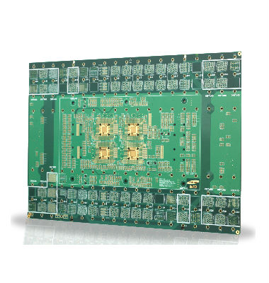
3. Stack-Up & Architecture Design
- Layer count definition (often 12–24+)
- Ground and power plane strategy
- Controlled impedance structures
4. Layout Implementation
- High pin count routing
- Length matching for timing-critical signals
- Crosstalk and EMI mitigation
5. Validation & Iteration
- SI/PI simulation
- Design for Manufacturability (DFM) review
- Prototype testing
This workflow ensures the final PCB is not only functional, but production-ready.
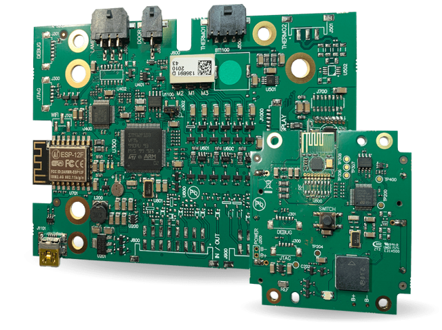
Critical Design Blocks
A successful custom ATE PCB is built around several key functional blocks:
- High-Speed Signal Routing
Supports DDR, PCIe, SerDes, or RF signals with strict impedance control - Power Distribution Network (PDN)
Delivers stable, low-noise power under dynamic test conditions - Socket Interface Region
Requires precise pad design, reinforcement, and flatness control - Connector & ATE Interface
Handles high-density connections with minimal signal degradation - Grounding & Shielding Structure
Ensures signal return paths and reduces interference
Each block must be optimized individually and as part of the overall system.
Risk & Failure Points
Custom ATE PCB projects often fail due to overlooked details. Key risks include:
- Signal Integrity Issues
Poor impedance control or via design can distort test signals - Power Instability
Weak PDN design leads to voltage drops and inaccurate results - Mechanical Misalignment
Improper flatness or tolerance affects socket contact reliability - Thermal Stress
Long test cycles can cause warpage or performance drift - Overdesign or Underdesign
Too complex → high cost and low yield
Too simple → insufficient performance
The key is balanced engineering, not maximum complexity.
Cost & Lead Time Drivers
Understanding cost and timeline early helps avoid project delays.
Main cost factors:
- Layer count and stack-up complexity
- Microvia and HDI usage
- Material selection (standard vs high-speed/low-loss)
- Surface finish (ENIG vs hard gold)
- Board size and panel utilization
Lead time drivers:
- Number of lamination cycles
- Fabrication complexity
- Prototype iterations
- Testing and validation cycles
Typical reality:
- Simple ATE board → 2–3 weeks
- Complex HDI ATE board → 3–6+ weeks
Early DFM collaboration with the manufacturer can significantly reduce both cost and lead time.
Final Thoughts
Custom ATE PCBs are not just test boards—they are precision-engineered systems that directly impact measurement accuracy, yield, and production efficiency.
Success depends on more than layout—it requires:
- System-level thinking
- Careful SI/PI optimization
- Manufacturing-aware design
- Balanced cost-performance decisions
At KKPCB, we support custom ATE PCB projects from initial specification through production, ensuring each design is optimized for accuracy, reliability, and scalability in real test environments.
