Role in Test Systems
A Multilayer Test PCB is a specialized board used in electronic testing environments, particularly in systems involving Automated Test Equipment (ATE), validation platforms, and high-speed signal verification.
Unlike standard PCBs, test boards are not part of the final product—they serve as temporary but critical platforms that ensure devices function correctly before deployment.
These PCBs are commonly used in:
- Semiconductor testing (IC validation and characterization)
- High-speed interface testing (DDR, PCIe, SerDes)
- Functional verification and debugging
- Burn-in and reliability testing systems
Their primary role is to provide a stable, repeatable, and accurate electrical environment for testing complex electronic components.
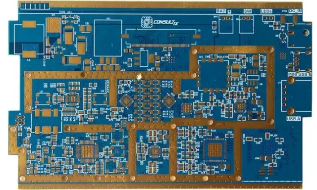
Design Architecture
Multilayer test PCBs are designed to handle high pin counts, dense routing, and multiple signal types simultaneously.
Key architectural elements include:
- High Layer Count Stack-Up:
Typically 8–20+ layers to separate signal, power, and ground planes, ensuring clean signal paths. - Controlled Impedance Routing:
Critical for maintaining signal fidelity in high-speed test scenarios. - Dedicated Ground Planes:
Provide stable reference paths and reduce noise and EMI. - Flexible Interface Design:
Supports sockets, connectors, and probe interfaces for various DUT configurations. - Modular Layout Approach:
Allows easy modification or reuse for different test scenarios.
This architecture ensures that the PCB supports accurate signal transmission without introducing distortion or instability.
Accuracy & Reliability Factors
In testing environments, accuracy is everything. Multilayer test PCBs must maintain:
- Signal Integrity (SI):
Minimizing reflection, insertion loss, and jitter ensures accurate measurement results. - Power Integrity (PI):
Stable voltage delivery is essential to avoid false test failures. - Repeatability:
Consistent performance across thousands of test cycles is required for production testing. - Thermal Stability:
Boards must maintain electrical performance under continuous operation and heat generation. - Mechanical Durability:
Frequent insertion/removal of components or sockets requires robust construction.
Any deviation in these factors can lead to incorrect test results, reduced yield, or misdiagnosis of device performance.
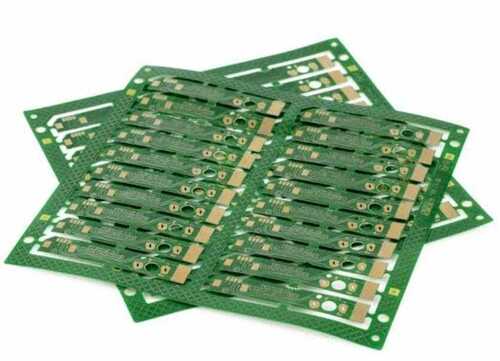
Manufacturing Requirements
Multilayer test PCBs require advanced fabrication processes and strict quality control:
- Precision Lamination:
Ensures layer alignment and structural integrity in complex stack-ups. - Fine Line & Spacing:
Supports high-density routing and high pin count devices. - Via Technologies:
Blind vias, buried vias, and microvias improve routing efficiency and signal performance. - Surface Finishes:
ENIG or hard gold finishes are preferred for durability and reliable electrical contact. - Quality Assurance:
- Impedance and continuity testing
- X-ray inspection for internal structures
- AOI for fine feature verification
- High-speed validation using TDR and VNA
At KKPCB, we ensure multilayer test PCBs meet strict electrical and mechanical requirements, supporting accurate and reliable testing environments.
When Should You Use a Multilayer Test PCB?
Multilayer test PCBs are essential when testing involves complex signals, high pin counts, or high-speed interfaces:
- IC validation and characterization
- High-speed digital interface testing
- RF and mixed-signal testing
- ATE and production test environments
- Reliability and burn-in testing
If your testing environment requires precision, stability, and repeatability, a multilayer test PCB is a critical component.
Final Thoughts
Multilayer test PCBs are not just test fixtures—they are precision platforms that directly impact test accuracy and production efficiency.
By combining high-layer-count design, controlled impedance routing, robust materials, and strict QA processes, KKPCB delivers Multilayer Test PCBs that ensure reliable and repeatable testing for advanced electronic systems.
