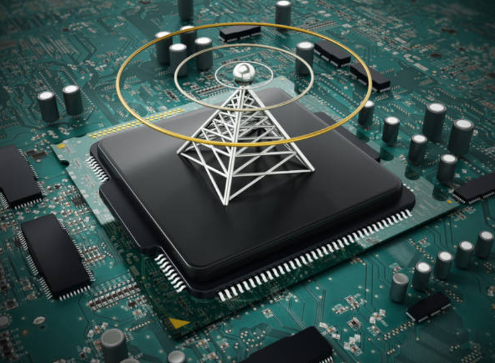
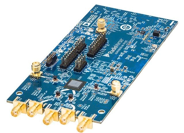
An RF Trace PCB is a printed circuit board optimized for radio frequency (RF) and microwave signals, typically operating from hundreds of MHz to several GHz. Unlike standard PCBs, RF trace boards must maintain signal integrity, controlled impedance, and minimal insertion loss across the board.
RF trace PCBs are widely used in:
-
Wireless communication systems (5G, Wi-Fi, LTE)
-
Satellite and aerospace electronics
-
Radar modules and RF amplifiers
-
High-speed networking and test equipment
The primary goal of an RF trace PCB is to ensure signals propagate accurately without reflection, distortion, or crosstalk, even at high frequencies.
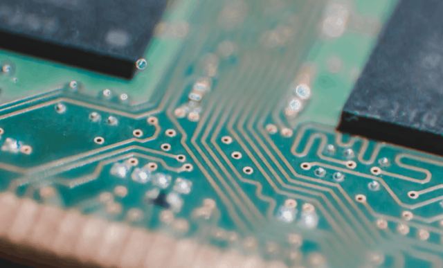
Design Challenges
Designing RF trace PCBs presents several technical challenges:
-
Signal Loss: High-frequency signals are prone to dielectric and conductor loss, which can reduce power efficiency and degrade signal quality.
-
Impedance Control: Inconsistent trace width, thickness, or laminate properties can cause impedance mismatches, resulting in signal reflections.
-
Crosstalk and EMI: Closely spaced traces and multilayer boards can induce electromagnetic interference between adjacent lines.
-
Thermal Effects: High-frequency operation generates heat, potentially altering the dielectric properties of the substrate.
-
Manufacturing Tolerances: Minor deviations in etching, lamination, or via placement can significantly impact RF performance.
Engineering Solutions
Engineers use multiple strategies to overcome these challenges:
-
Controlled Impedance Traces: Designing microstrip, stripline, or coplanar waveguide traces to maintain precise impedance.
-
Trace Geometry Optimization: Minimizing trace length, avoiding sharp bends, and using gradual transitions reduce reflections and signal loss.
-
Differential Signaling: Where possible, differential pairs improve noise immunity and reduce EMI.
-
Shielding and Grounding: Ground planes, vias, and guard traces isolate high-frequency signals from noisy sections.
-
Thermal Management: Copper pours, thermal vias, and careful layer stack-ups help dissipate heat in densely routed high-frequency circuits.
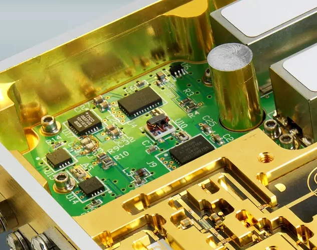
Materials & Fabrication
High-quality materials and precise fabrication are crucial for RF trace PCBs:
-
Low-Loss Laminates: PTFE-based, ceramic-filled, or Taconic laminates minimize dielectric loss and stabilize Dk.
-
Precision Drilling and Plating: Microvias and through-holes are manufactured to prevent impedance discontinuities.
-
Surface Finishes: ENIG, hard-gold, or immersion silver optimize solderability and reduce signal reflection.
-
Quality Assurance:
-
Impedance testing and Vector Network Analysis (VNA) measure insertion and return loss
-
AOI/X-ray inspections verify trace and via integrity
-
Thermal cycling ensures stability under operational stress
-
KKPCB leverages advanced fabrication and QA to deliver RF trace PCBs with reliable high-frequency performance.
Applications
RF trace PCBs are essential for modern electronics where high-frequency signal fidelity is critical:
-
Wireless Communication: Antennas, RF front-end modules, and 5G infrastructure
-
Satellite and Aerospace Systems: Radar modules, transceivers, and satellite communication circuits
-
High-Speed Networking: Data routers, switches, and RF transmission boards
-
Test & Measurement Equipment: RF diagnostic and signal analysis instruments
-
Microwave Modules: Amplifiers, mixers, and filters operating at GHz frequencies
By integrating precise trace design, low-loss laminates, controlled impedance, and rigorous QA, KKPCB delivers RF Trace PCBs capable of maintaining signal integrity and performance in demanding high-frequency applications.
