What is a High Frequency Laminate PCB?
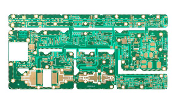
A High Frequency Laminate PCB is a printed circuit board built with specialized substrate materials optimized for low dielectric loss (Df), stable dielectric constant (Dk), and high thermal performance at high frequencies. Unlike standard FR-4, high frequency laminates maintain signal integrity in RF, microwave, and high-speed digital applications, minimizing signal degradation and reflection.
Common high frequency laminates include:
-
Rogers Materials (e.g., RO3000, RO4000 series): Excellent for RF/microwave circuits
-
PTFE-based Laminates: Ultra-low loss for mmWave applications
-
Ceramic-filled Laminates: Balances thermal performance and signal integrity
These laminates are essential wherever signals operate at hundreds of MHz up to several GHz and require consistent impedance and low attenuation.
High Frequency Laminate PCB Design
Designing high frequency laminate PCBs requires attention to electrical, thermal, and mechanical considerations:
-
Controlled Impedance:
Maintaining precise impedance is critical for signal integrity. Trace width, spacing, laminate thickness, and Dk must be carefully calculated. Microstrip, stripline, and coplanar waveguide designs are common for high-frequency routing. -
Minimizing Loss:
Low Df materials reduce dielectric and conductor losses. Designers optimize trace geometry, minimize via stubs, and use short signal paths to maintain high-frequency performance. -
Thermal Management:
High-speed circuits often generate significant heat. Laminates with higher thermal conductivity, combined with copper pours and thermal vias, help dissipate heat efficiently, ensuring stable operation. -
Layer Stack-Up Planning:
Multilayer stack-ups balance RF signal layers, power distribution, and grounding. Careful layer allocation reduces crosstalk and EMI while preserving high-speed performance. -
Material Selection:
Material choice depends on frequency range, loss requirements, and operating temperature. PTFE and ceramic-filled laminates are preferred for mmWave or high-power applications, while Rogers laminates suit most RF/microwave circuits.
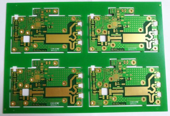
Manufacturing Considerations and QA
Fabrication of high frequency laminate PCBs involves precision processes:
-
Accurate Drilling and Plating: Via quality is critical; laser or mechanical drilling ensures precision without damaging the substrate.
-
Controlled Lamination: Ensures layer alignment and consistent dielectric thickness, crucial for impedance control.
-
Surface Finishes: ENIG, hard-gold, or immersion silver are selected based on RF performance and solderability.
-
Inspection and Testing:
-
Impedance verification for critical RF traces
-
Vector Network Analysis (VNA) for insertion loss and return loss
-
AOI and X-ray inspection for multilayer quality and via integrity
-
KKPCB applies these advanced techniques to consistently produce high frequency laminate PCBs with reliable performance across demanding applications.
Applications of High Frequency Laminate PCBs
High frequency laminate PCBs are widely used where high-speed signal fidelity is critical:
-
5G and Wireless Communication: RF front-end modules, antennas, and base stations
-
Satellite and Aerospace Electronics: Radar systems, transceivers, and high-frequency communication modules
-
High-Speed Networking: Data routers, switches, and GHz-level transmission circuits
-
Test & Measurement Equipment: High-frequency measurement and diagnostic instruments
-
RF Amplifiers and Microwave Modules: Maintaining low-loss performance at high frequencies
By combining advanced laminate materials, precise layout, thermal optimization, and strict QA processes, KKPCB delivers high frequency laminate PCBs capable of reliable operation in demanding RF, microwave, and high-speed digital environments.
