What is an RF Trace PCB?
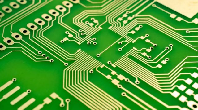
An RF Trace PCB is a printed circuit board specifically designed to handle high-frequency radio frequency (RF) signals, typically ranging from MHz to GHz and even mmWave frequencies. Unlike standard PCB traces, RF traces must be carefully engineered to behave as controlled transmission lines, ensuring signals propagate with minimal reflection, loss, and distortion.
RF trace design is fundamental in applications such as wireless communication, radar systems, satellite modules, and high-speed networking devices. At high frequencies, even small variations in trace geometry, dielectric properties, or layout can significantly impact performance.
RF Trace PCB Design
Designing RF trace PCBs requires a deep understanding of electromagnetic behavior and transmission line theory:
-
Controlled Impedance Design:
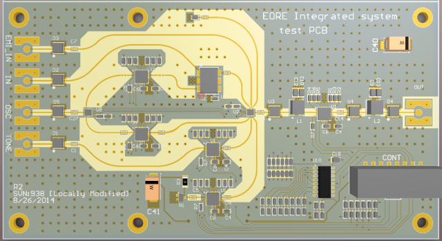
RF traces must maintain consistent impedance (commonly 50Ω or 75Ω). This depends on trace width, substrate thickness, dielectric constant (Dk), and copper thickness. Microstrip and stripline structures are commonly used to achieve precise impedance control. -
Transmission Line Structures:
-
Microstrip: Trace on the outer layer with a reference ground plane beneath
-
Stripline: Trace embedded between two ground planes for better shielding
Each structure offers different trade-offs between loss, shielding, and manufacturability.
-
Minimizing Signal Loss:
Signal loss in RF PCBs comes from dielectric loss and conductor loss. Designers use smooth copper surfaces, optimized trace geometry, and low-loss materials to reduce attenuation, especially at higher frequencies. -
Crosstalk and EMI Control:
Proper spacing between RF traces, continuous ground planes, and via shielding techniques are used to reduce electromagnetic interference (EMI). Guard traces and ground vias can further isolate sensitive RF signals. -
Via and Transition Design:
Vias introduce impedance discontinuities and parasitic inductance. In RF designs, vias must be minimized or carefully optimized using back-drilling or via stubs removal techniques. -
Material Selection:
Low-loss materials such as PTFE-based laminates, Rogers materials, or advanced low-Df substrates are essential for maintaining signal integrity in high-frequency applications.
Manufacturing Considerations and QA
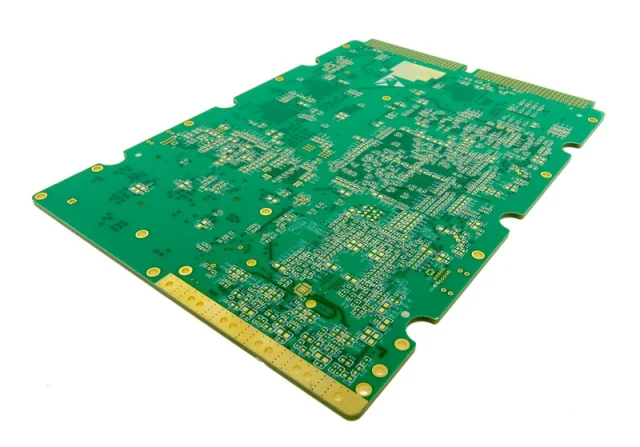
RF Trace PCBs demand extremely tight process control during fabrication:
-
Precision Etching: Even slight variations in trace width can affect impedance and signal performance.
-
Dielectric Thickness Control: Consistency in substrate thickness is critical for impedance accuracy.
-
Smooth Copper Foil: Reduces conductor loss, especially at high frequencies.
-
Lamination Accuracy: Ensures consistent layer spacing and alignment in multilayer RF boards.
Quality assurance is essential for RF performance validation:
-
Impedance Testing: Confirms traces meet target impedance values.
-
Time Domain Reflectometry (TDR): Detects impedance discontinuities along RF traces.
-
Vector Network Analysis (VNA): Measures insertion loss, return loss, and overall RF performance.
-
AOI and X-ray Inspection: Ensures structural and internal integrity of the PCB.
KKPCB applies advanced fabrication techniques and rigorous testing to ensure RF trace PCBs meet strict high-frequency performance requirements.
Applications of RF Trace PCBs
RF trace PCBs are essential in high-frequency and communication systems:
-
5G and Wireless Communication: Supporting antennas, RF front-end modules, and base stations
-
Radar and Aerospace Systems: Enabling precise signal transmission in harsh environments
-
Satellite Communication: Maintaining signal integrity over long distances
-
High-Speed Networking Equipment: Supporting GHz-level data transmission
As modern electronics continue to push toward higher frequencies and faster data rates, RF trace PCB design becomes increasingly critical. With expertise in controlled impedance, low-loss materials, and precision manufacturing, KKPCB delivers RF PCB solutions that ensure stable, high-performance signal transmission.
