Power Integrity PCB: Ensuring Stable Power Delivery for High-Speed Electronics
As modern electronic systems operate at increasingly high speeds, maintaining Power Integrity (PI) on printed circuit boards is critical. Power Integrity PCB design ensures that all components receive clean, stable voltage, minimizing noise, voltage drop, and electromagnetic interference (EMI). Poor power integrity can cause timing errors, signal degradation, and system instability, making PI a key consideration in high-speed digital and RF PCB design.
This article explains the fundamentals, design strategies, and best practices for power integrity in PCB design, helping engineers achieve reliable performance in complex electronic systems.
What Is Power Integrity in PCB Design?
Power Integrity refers to the ability of a PCB’s power distribution network (PDN) to maintain stable voltage across all components under dynamic operating conditions. High-speed ICs and processors draw rapid transient currents that can cause voltage fluctuations, impacting overall system performance.
Key goals of power integrity include:
-
Stable voltage supply across all components
-
Minimal noise and ripple on power planes
-
Low impedance in power distribution networks
-
Enhanced reliability of high-speed circuits
A Power Integrity PCB ensures the PDN can handle fast current changes while maintaining consistent power delivery.
Why Power Integrity Is Critical
High-speed electronics are highly sensitive to voltage fluctuations. Without proper PI design, issues can include:
-
Signal integrity degradation
-
Increased electromagnetic interference (EMI)
-
Timing and synchronization errors
-
Reduced reliability and component lifespan
Power integrity is particularly important in:
-
High-performance computing (HPC) systems
-
5G and networking equipment
-
Automotive electronics
-
High-speed memory and FPGA designs
Key Power Integrity PCB Design Strategies

1. Optimized Power Distribution Network (PDN)
A robust PDN ensures low impedance across the frequency range. Techniques include:
-
Wide power and ground planes
-
Short current paths from source to load
-
Layer stacking to reduce loop inductance
2. Decoupling Capacitor Placement
Decoupling capacitors stabilize voltage and filter high-frequency noise. Best practices:
-
Place capacitors close to IC power pins
-
Use multiple capacitor values for broadband decoupling
-
Minimize loop inductance by routing directly between capacitor and power pin
3. Multilayer PCB Stackup Optimization
Layering impacts both power integrity and signal integrity. Effective strategies:
-
Dedicated power and ground plane pairs
-
Symmetrical stackups to reduce warpage
-
Adjacent planes to create natural decoupling capacitance
4. Minimize Power Plane Discontinuities
Splits or gaps in power planes increase impedance and degrade PI. Continuous power planes help maintain stable current flow and reduce voltage fluctuations.
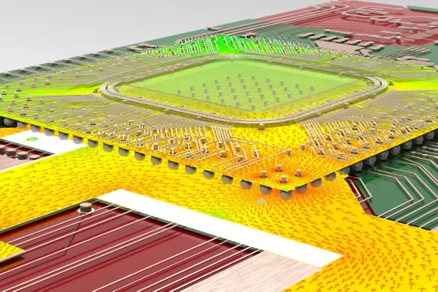
5. Power Integrity Simulation
Simulation tools allow engineers to:
-
Analyze PDN impedance and resonances
-
Predict voltage drops and ripple under load
-
Optimize decoupling strategies before fabrication
Applications of Power Integrity PCB
Power integrity design is essential in:
-
Data center servers and networking equipment
-
High-speed memory and FPGA boards
-
AI and GPU computing hardware
-
Automotive electronics and EV control systems
-
Telecommunication infrastructure
-
Industrial automation systems
In all these applications, stable power ensures reliable operation of high-speed and high-performance circuits.
Power Integrity vs Signal Integrity

While signal integrity focuses on accurate signal propagation, power integrity ensures voltage stability. Both must be considered together in modern PCB design to prevent data errors and system instability.
Conclusion
Designing a Power Integrity PCB is essential for high-speed and high-performance electronics. By optimizing power distribution networks, strategically placing decoupling capacitors, maintaining continuous power planes, and simulating PDN performance, engineers can ensure stable power delivery and improve overall system reliability.
As devices continue to operate at higher speeds and densities, power integrity will remain a fundamental aspect of advanced PCB design.
