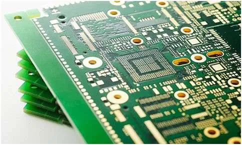
What Is a Buried Via PCB?
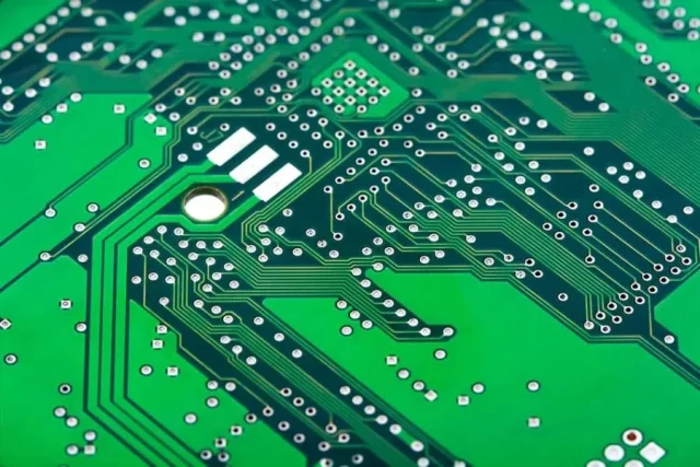
A Buried Via PCB is a type of multilayer printed circuit board that uses buried vias to connect internal copper layers without reaching the outer surface layers. Unlike through-hole vias that pass through the entire board, buried vias exist only between inner layers, remaining invisible from the exterior of the PCB.
This technology allows designers to maximize routing space on the outer layers while maintaining complex internal connections. Buried via PCBs are commonly used in high-density electronic products where space optimization and signal integrity are critical.
These PCBs are widely applied in industries such as:
-
High-speed communication equipment
-
Advanced computing systems
-
Aerospace electronics
-
Medical devices
-
Consumer electronics with compact designs
By embedding the vias inside the board structure, engineers can achieve higher circuit density and improved electrical performance.
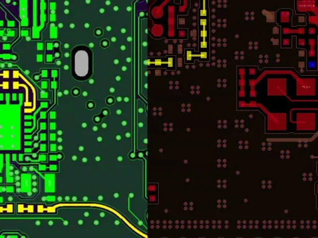
Structure of Buried Via PCBs
Buried vias are created during the multilayer lamination process and connect two or more internal layers within the PCB stack-up. Because they do not reach the outer layers, additional lamination steps are typically required during manufacturing.
A typical buried via PCB structure may include:
-
Outer signal layers for component mounting
-
Inner signal layers for routing
-
Power and ground planes for stable electrical performance
-
Buried vias connecting specific internal layers
This layered architecture allows designers to optimize routing paths while preserving valuable surface area.
Advantages of Buried Via PCB
Higher Routing Density
Buried vias free up space on outer layers, enabling designers to place more components and routes in compact circuit layouts.
Improved Signal Integrity
By shortening signal paths and reducing via stubs, buried vias help minimize signal reflection and interference, which is especially important in high-speed circuits.
Better Space Utilization
Without visible via pads on the outer layers, the board surface becomes more available for component placement and fine routing.
Enhanced Design Flexibility
Designers can create more efficient multilayer structures by strategically connecting internal layers without affecting surface routing.
Design Considerations for Buried Via PCBs
Designing a buried via PCB requires careful planning to ensure manufacturability and reliability.
Layer Stack-Up Planning
Proper stack-up design determines which internal layers will be connected by buried vias and how the board will be laminated.
Manufacturing Complexity
Buried via PCBs require sequential lamination processes, increasing manufacturing precision and production complexity compared to standard PCBs.
Thermal Reliability
Internal vias must be carefully designed to maintain mechanical strength and avoid reliability issues during thermal cycling.
Signal Routing Optimization
Buried vias are often used together with blind vias and microvias to support advanced high-density interconnect (HDI) PCB designs.
Applications of Buried Via PCBs
Buried via PCBs are commonly used in modern electronics that demand compact size, high circuit density, and reliable signal performance.
Typical applications include:
-
High-speed networking hardware
-
5G communication equipment
-
Advanced computing motherboards
-
Aerospace and defense systems
-
Medical imaging electronics
These applications require sophisticated multilayer boards capable of handling complex circuit routing within limited space.
Conclusion
A Buried Via PCB is an advanced multilayer circuit board technology that improves routing efficiency and enables high-density electronic designs. By embedding vias inside the PCB structure, designers can optimize board space, enhance signal performance, and support increasingly complex electronic systems.
As electronic devices continue to become smaller and more powerful, buried via technology will play an increasingly important role in high-performance PCB manufacturing.
