What Is a High Frequency Sensor PCB?
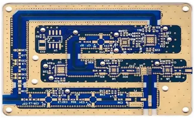
A High Frequency Sensor PCB is a specialized printed circuit board engineered to support sensors operating in RF and microwave frequency ranges. These boards are designed to maintain signal accuracy, minimize transmission loss, and ensure stable performance under demanding environmental conditions.
High-frequency sensors are widely used in:
-
Radar detection systems
-
Industrial monitoring equipment
-
Medical diagnostic devices
-
Wireless sensing modules
-
Environmental detection systems
Because sensor signals are often weak and highly sensitive to interference, PCB design plays a critical role in overall system accuracy.
Key Design Considerations
1. Low-Loss Material Selection
At high frequencies, dielectric loss directly affects signal strength and measurement precision.
To reduce insertion loss and phase distortion, designers commonly use low-loss laminates supplied by companies such as Rogers Corporation or Taconic.
Important material properties include:
-
Low dielectric constant (Dk) variation
-
Low dissipation factor (Df)
-
Stable thermal performance
-
Consistent electrical characteristics across frequency ranges
Material stability ensures predictable sensor calibration.
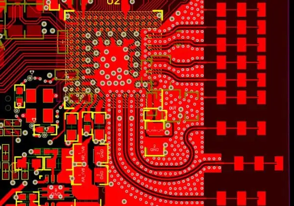
2. Controlled Impedance Routing
High-frequency sensor circuits require precise impedance control to maintain signal integrity.
Design techniques include:
-
Microstrip or stripline routing
-
Tight trace width tolerance
-
Proper ground referencing
-
Minimized via transitions
Any impedance mismatch can cause signal reflection, leading to inaccurate sensor readings.
3. Noise and EMI Suppression
Sensor circuits are highly sensitive to noise. Effective PCB layout must:
-
Separate analog and digital domains
-
Maintain continuous ground planes
-
Minimize loop areas
-
Implement shielding where necessary
Proper isolation prevents electromagnetic interference from corrupting weak RF signals.
4. Thermal Stability
Temperature fluctuations can shift sensor performance. High-frequency sensor PCBs are often designed with:
-
Low CTE materials
-
Balanced multilayer stack-up
-
Stable dielectric properties over temperature range
Thermal stability is essential for industrial and outdoor sensor systems.
Multilayer Structure and Miniaturization
Modern sensing systems require compact form factors. High Frequency Sensor PCBs may feature:
-
Multilayer construction
-
Blind or buried vias
-
Fine trace geometry
-
Dense RF component integration
These features enable compact modules without sacrificing performance.
Typical Applications
High Frequency Sensor PCBs are commonly found in:
-
Automotive radar modules
-
Industrial level and motion detection systems
-
Wireless IoT sensor nodes
-
Aerospace monitoring devices
-
Medical imaging equipment
In each application, signal precision and reliability are critical.
High Frequency Sensor PCB vs Standard Sensor PCB
| Feature | Standard Sensor PCB | High Frequency Sensor PCB |
|---|---|---|
| Frequency Range | Low–Medium | RF & Microwave |
| Material Type | FR4 | Low-Loss RF Laminate |
| Signal Sensitivity | Moderate | Very High |
| EMI Control | Basic | Advanced |
| Calibration Stability | Standard | High Precision |
High Frequency Sensor PCBs are optimized for signal accuracy, stability, and low transmission loss.
Conclusion
A High Frequency Sensor PCB is a critical foundation for RF and microwave sensing systems.With low-loss materials, controlled impedance routing, advanced EMI suppression, and thermal stability, these PCBs ensure accurate signal detection and long-term reliability.As sensing technologies continue to advance in automotive, industrial, and medical applications, precision PCB design remains essential for maintaining system performance.
