What Is a High Frequency Sensor PCB?
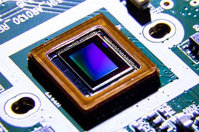
A High Frequency Sensor PCB is a printed circuit board designed specifically for high-speed sensors that operate in the MHz to GHz frequency range. These PCBs are optimized for:
-
Minimal signal attenuation
-
High signal integrity
-
Accurate data acquisition
They are widely used in radar sensors, LiDAR modules, RF sensing devices, and industrial measurement systems.
Key Features of High Frequency Sensor PCB
1. Low-Loss Materials
High-frequency sensor PCBs typically use low-loss laminates such as:
-
Rogers Corporation
-
Taconic
These materials provide:
-
Low dielectric loss (Df)
-
Stable dielectric constant (Dk)
-
Reliable performance in high-frequency applications
Low-loss materials are critical for sensors that rely on precise timing and signal strength.
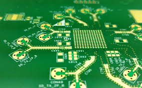
2. Controlled Impedance and Signal Integrity
High-frequency sensor PCBs require precise impedance control to:
-
Minimize reflection and insertion loss
-
Ensure accurate signal propagation
-
Maintain synchronization between sensor elements
Multilayer stack-ups with dedicated ground planes and RF routing layers are commonly used.
3. High-Speed Data Transmission
Sensor modules often integrate with digital processors or communication interfaces that require:
-
High-speed serial data lines
-
Differential pair routing
-
Shielding for sensitive analog signals
Proper layout ensures reliable signal acquisition and minimal data errors.
4. Thermal and Mechanical Reliability
High-frequency sensors may operate in:
-
Industrial environments with temperature variations
-
Automotive systems exposed to vibration
-
Aerospace modules with thermal cycling
PCB design includes:
-
High Tg substrates
-
Reinforced vias
-
Efficient thermal management strategies
These measures guarantee long-term stability and durability.
5. EMI/EMC Considerations
High-frequency sensor PCBs often coexist with other electronics, so EMI and EMC control is essential:
-
Ground and power plane separation
-
Filter networks on sensitive lines
-
Shielding vias and controlled layer separation
Effective EMI management improves measurement accuracy and sensor reliability.
Applications of High Frequency Sensor PCB
-
Automotive radar and LiDAR sensors
-
Industrial RF measurement devices
-
Wireless sensor networks (IoT modules)
-
Aerospace navigation and positioning sensors
-
Medical imaging and monitoring equipment
The combination of high-frequency performance, low-loss material, and signal integrity ensures precise and reliable sensor operation.
High Frequency Sensor PCB vs Standard Sensor PCB
| Feature | Standard Sensor PCB | High Frequency Sensor PCB |
|---|---|---|
| Frequency Range | kHz–MHz | MHz–GHz |
| Material | FR4 | Low-loss RF laminates |
| Signal Integrity | Moderate | High |
| Impedance Control | Basic | Precise |
| EMI/EMC | Moderate | Advanced |
| Thermal/Vibration Resistance | Standard | High |
High-frequency sensor PCBs are critical when timing, data accuracy, and signal fidelity cannot be compromised.
Conclusion
High Frequency Sensor PCBs are engineered for low-loss, high-speed signal processing in precision sensing applications. With controlled impedance, thermal reliability, and EMI mitigation, these PCBs ensure accurate data acquisition and reliable sensor performance.
For applications in automotive radar, LiDAR, aerospace, industrial IoT, and medical devices, high-frequency sensor PCBs are essential for precision, reliability, and high-speed operation.
