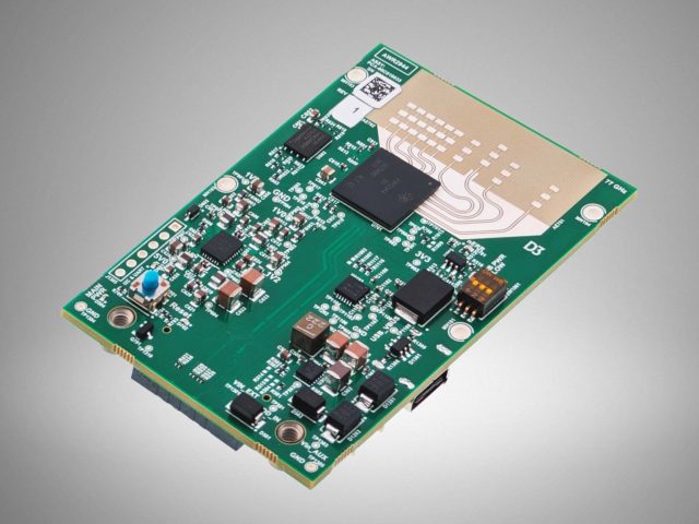
What Is an ADAS PCB?

An ADAS PCB is a specialized printed circuit board designed for Advanced Driver Assistance Systems in modern vehicles. These PCBs serve as the backbone for integrating multiple sensors, controllers, and communication modules, enabling functions such as lane departure warning, adaptive cruise control, collision avoidance, and autonomous driving support.
Unlike standard automotive PCBs, ADAS PCBs must handle high-speed signal processing, strict EMI/EMC requirements, and operate reliably under extreme automotive conditions.
Key Features of ADAS PCB
1. Multi-Sensor Integration
ADAS systems combine data from:
-
Cameras
-
LiDAR sensors
-
Radar modules
-
Ultrasonic sensors
PCB layout must support multiple high-speed interfaces while keeping signal integrity intact.
2. High-Speed Data Transmission
Sensors and ECUs communicate using:
-
CAN / CAN-FD
-
Ethernet (Automotive 100/1000Base-T1)
-
FlexRay
-
High-speed serial interfaces
Controlled impedance and low-loss materials are crucial to reduce signal reflection and maintain reliable timing.
3. Automotive-Grade Reliability
Automotive PCBs, including ADAS PCB, must withstand:
-
Wide temperature ranges (-40°C to 125°C)
-
Vibration and mechanical shock
-
Moisture and humidity
-
Thermal cycling
High TG materials, reinforced vias, and multilayer stack-ups improve mechanical and thermal stability.
4. EMI / EMC Considerations
Automotive environments are electrically noisy. ADAS PCB design must include:
-
Proper grounding and shielding
-
Segregation of analog, digital, and RF traces
-
Filter networks for sensitive signals
-
Controlled return paths for high-speed interfaces
Effective EMI management ensures sensors and controllers operate accurately.
5. Thermal Management
ADAS modules often include:
-
Image processors
-
AI accelerators
-
Power management ICs
Efficient thermal design, including thick copper layers, thermal vias, and optimized heat dissipation paths, is critical for long-term reliability.
Typical ADAS PCB Structures
-
Multilayer PCB – 6–12 layers for power, signal, and ground planes
-
HDI PCB – For compact sensor and processor boards
-
Rigid-Flex PCB – To connect modules in tight automotive assemblies
-
High TG / Low Loss Materials – For thermal stability and high-speed signaling
The stack-up is designed to balance electrical performance, mechanical durability, and automotive reliability standards.
Applications of ADAS PCB
ADAS PCBs are widely used in:
-
Autonomous driving ECUs
-
Lane departure warning systems
-
Adaptive cruise control modules
-
Collision avoidance and braking systems
-
Parking assistance controllers
-
Surround view camera systems
High integration and reliability are key for safety-critical automotive applications.
ADAS PCB vs Standard Automotive PCB
| Feature | Standard Automotive PCB | ADAS PCB |
|---|---|---|
| Signal Speed | Moderate | High |
| Multi-Sensor Integration | Limited | Extensive |
| EMI/EMC Control | Basic | Advanced |
| Thermal Management | Standard | Critical |
| Mechanical Robustness | Standard | Enhanced |
ADAS PCB design focuses on high-speed signal fidelity, safety, and long-term reliability.
Conclusion
ADAS PCB technology enables modern vehicles to safely and reliably process multiple sensor inputs and control advanced driver assistance functions. Through careful multilayer design, high-speed signal optimization, thermal and mechanical management, and EMI/EMC strategies, ADAS PCBs ensure robust performance under harsh automotive conditions.
For the future of autonomous and semi-autonomous vehicles, ADAS PCB serves as the central platform supporting safe, reliable, and intelligent driving functions.
