What Is a Probe Card PCB?
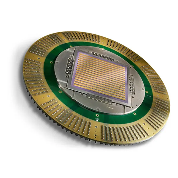
A Probe Card PCB is a high-precision printed circuit board used in semiconductor wafer-level testing. It serves as the electrical interface between Automated Test Equipment (ATE) systems and the wafer under test.
Unlike load boards used for packaged ICs, probe card PCBs are specifically designed to connect to microscopic probe needles or MEMS probe arrays that contact semiconductor wafers before packaging.
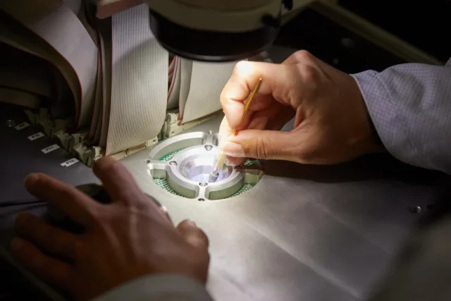
Probe card PCBs play a critical role in wafer sort and early defect screening.
The Role of Probe Card PCB in Wafer Testing
During wafer-level testing, each die on the wafer must be electrically verified before it proceeds to packaging. The probe card PCB enables:
-
Signal transmission between ATE and wafer
-
Power delivery to test dies
-
High-speed data routing
-
Parametric measurement support
-
RF characterization
Because wafer-level testing happens before packaging, accuracy at this stage directly affects yield and cost efficiency.
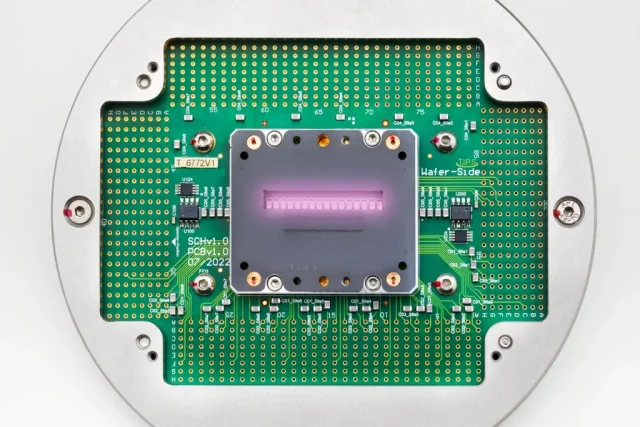
Key Design Challenges
1. Ultra-High Interconnection Density
Modern wafers contain high pin-count devices with extremely fine pitch pads. The PCB must support:
-
Microvia structures
-
HDI routing
-
Fine line geometry
-
Tight registration control
High-density interconnect design is essential.
2. High-Frequency and High-Speed Compatibility
Advanced semiconductor devices often require:
-
GHz-level signal routing
-
Differential pair control
-
Low insertion loss
-
Stable impedance
Low-loss materials and controlled stack-up design ensure measurement accuracy.
3. Mechanical Stability and Planarity
Probe card PCBs must maintain:
-
Flatness under temperature variation
-
Stable alignment with probe assemblies
-
Mechanical durability under repeated contact cycles
Material stability and symmetrical stack-up are critical for long-term performance.
4. Thermal Management
During wafer testing, power devices may generate heat. Probe card PCBs incorporate:
-
Copper planes for heat spreading
-
Thermal vias
-
Optimized layout for temperature balance
This prevents measurement drift caused by thermal expansion.
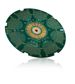
Structural Features
Probe card PCBs often include:
-
Multilayer stack-ups
-
Microvias and buried vias
-
Controlled impedance routing
-
Precision connector interfaces
-
Reinforced mounting areas
Advanced boards may combine rigid and specialized support materials to improve mechanical rigidity.
Applications of Probe Card PCB
Probe card PCBs are widely used in:
-
Wafer sort testing
-
RF chip wafer validation
-
Memory device testing
-
Automotive semiconductor qualification
-
AI and high-performance processor wafers
-
Power device wafer screening
They are essential in ensuring only known-good dies move to packaging.
Probe Card PCB vs Load Board PCB
| Feature | Probe Card PCB | Load Board PCB |
|---|---|---|
| Testing Stage | Wafer level | Packaged IC |
| Contact Method | Probe needles / MEMS | Test socket |
| Density Requirement | Extremely High | High |
| Mechanical Precision | Critical | High |
| Role in Production | Early defect screening | Final functional testing |
Probe card PCBs operate earlier in the semiconductor manufacturing flow and require tighter mechanical precision.
Conclusion
Probe Card PCB technology is fundamental to wafer-level semiconductor testing. With high-density routing, stable mechanical performance, and precise impedance control, it ensures accurate electrical validation before packaging.
As semiconductor nodes continue to shrink and signal speeds increase, probe card PCB design must meet even stricter electrical and mechanical performance standards.
