ATE Test PCB for Semiconductor and IC Testing
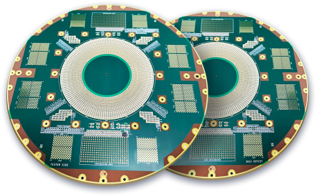
An ATE Test PCB (Automated Test Equipment PCB) is a high-precision printed circuit board designed for semiconductor and integrated circuit testing systems. It serves as the electrical interface between the test system and the device under test (DUT), ensuring accurate signal transmission, stable power delivery, and reliable long-term operation.
ATE systems demand extremely high electrical performance, tight mechanical tolerances, and stable impedance control. Therefore, ATE Test PCB manufacturing requires advanced fabrication capabilities and strict quality control.
Key Requirements of ATE Test PCB
1. High Signal Integrity
ATE boards often support:
-
High-speed digital signals
-
High-frequency RF signals
-
Mixed-signal testing environments
To maintain signal accuracy, ATE Test PCBs require:
-
Controlled impedance routing
-
Differential pair matching
-
Low insertion loss materials
-
Minimal via stubs (back drilling or microvias)
Signal integrity directly impacts test accuracy and repeatability.
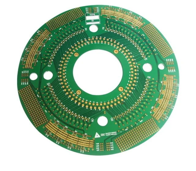
2. High Pin Count & Dense Routing
Modern IC packages such as BGA, QFN, and CSP demand:
-
Fine pitch routing
-
HDI structures
-
Blind and buried vias
-
Microvia technology
High layer count (8–24+ layers) is common in complex ATE load boards.
3. Stable Power Distribution
ATE systems require precise voltage control. PCB design must ensure:
-
Low resistance power planes
-
Heavy copper for high current testing
-
Stable grounding structure
-
Reduced noise coupling
Accurate power delivery ensures reliable test results.
4. Mechanical Precision
ATE Test PCBs must maintain:
-
Tight dimensional tolerance
-
Accurate alignment with test sockets
-
Minimal warpage
Mechanical stability is critical for consistent contact between DUT and test interface.
5. Thermal Management
High power test conditions may generate heat. ATE PCBs may include:
-
Thermal vias
-
Copper balancing
-
High TG materials
-
Metal reinforcement structures
Thermal control ensures long-term reliability during continuous testing cycles.
Types of ATE Test PCBs
ATE-related boards typically include:
-
Load boards
-
Probe interface boards
-
Burn-in boards
-
Logic test boards
-
RF test boards
Each type has specific electrical and structural requirements depending on test environment and device type.
Applications of ATE Test PCB
ATE Test PCBs are widely used in:
-
Semiconductor wafer testing
-
IC package testing
-
Automotive chip validation
-
RF device testing
-
High-speed processor testing
-
Memory testing
With increasing chip complexity and higher data rates, ATE PCB technology continues to evolve.
Manufacturing Capabilities for ATE Test PCB
Professional ATE PCB fabrication may include:
-
8–30+ layer multilayer structures
-
HDI microvia processing
-
Controlled impedance verification
-
Back drilling
-
Low loss and high TG materials
-
X-ray and AOI inspection
-
100% electrical testing
Strict process control ensures consistent quality across test cycles.
ATE Test PCB vs Standard PCB
| Feature | Standard PCB | ATE Test PCB |
|---|---|---|
| Precision Level | Commercial | High Precision |
| Layer Count | Moderate | High |
| Impedance Control | Optional | Strict |
| Mechanical Tolerance | Standard | Tight |
| Reliability Requirement | Normal | Critical |
ATE Test PCBs are engineered for performance stability and test accuracy rather than general-purpose electronics.
Conclusion
ATE Test PCB plays a critical role in semiconductor and electronic device validation. With high layer count structures, HDI technology, controlled impedance routing, and strict fabrication tolerance, these PCBs ensure precise and reliable testing results.
As semiconductor devices become faster and more complex, high-performance ATE Test PCB solutions are essential for maintaining testing accuracy and operational efficiency.
