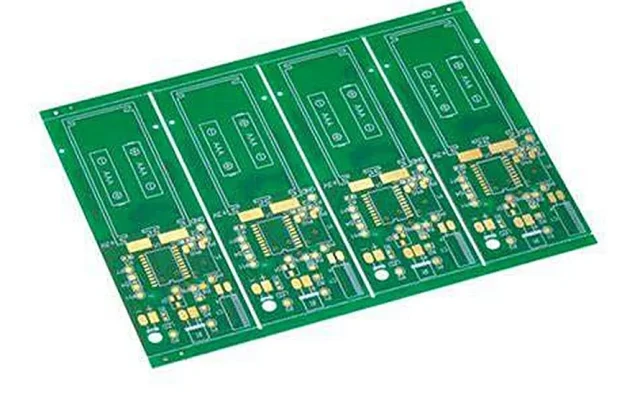
Double Layer HF PCB for RF and Microwave Systems
A Double Layer HF PCB (High Frequency PCB) is a two-layer printed circuit board designed specifically for RF and microwave signal transmission. Unlike standard double-sided FR4 boards, HF PCBs use low-loss, stable dielectric materials to ensure reliable signal performance at high frequencies.
Double layer high frequency boards are widely used in RF modules, antenna systems, radar units, and wireless communication devices where signal integrity and impedance stability are critical.
Why Choose a Double Layer HF PCB?
While multilayer RF boards are common in complex systems, double layer structures offer several advantages:
-
Lower manufacturing cost
-
Shorter production cycle
-
Simpler stack-up design
-
Reduced insertion loss (fewer dielectric interfaces)
-
Easier impedance control
For many RF front-end modules and antenna designs, a properly engineered two-layer high frequency PCB is both efficient and cost-effective.
Key Design Considerations
1. Low Loss Dielectric Materials
High frequency performance depends heavily on substrate properties. HF PCBs typically use:
-
Low dielectric constant (Dk) materials
-
Low dissipation factor (Df) laminates
-
Stable dielectric performance across frequency
Material selection directly affects insertion loss and signal stability.
2. Controlled Impedance Routing
Double layer HF PCB design often includes:
-
50Ω microstrip transmission lines
-
Coplanar waveguide (CPWG) structures
-
Ground plane optimization
-
Tight tolerance trace width control
Accurate impedance control ensures minimal signal reflection.
3. Grounding and EMI Management
In two-layer RF boards, grounding strategy is critical. Design typically includes:
-
Continuous ground plane on one side
-
Via stitching for ground stability
-
Isolation between RF and power sections
Proper grounding reduces noise and improves radiation performance.
4. Surface Finish Selection
For high frequency applications, surface finish impacts signal quality. Common finishes include:
-
ENIG
-
Immersion silver
These finishes provide smooth copper surfaces that reduce conductor loss at high frequencies.
Applications of Double Layer HF PCB
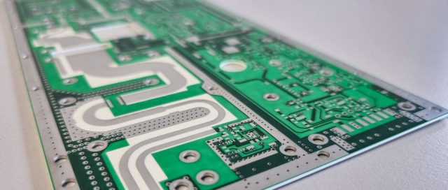
Double layer HF PCBs are commonly used in:
-
RF front-end modules
-
Antenna boards
-
2.4GHz / 5.8GHz wireless modules
-
IoT communication devices
-
Radar sensor modules
-
Satellite communication components
-
GPS modules
For compact RF modules, two-layer high frequency PCBs offer excellent performance-to-cost balance.
Double Layer HF PCB vs Standard Double-Sided PCB
| Feature | Standard Double Layer PCB | Double Layer HF PCB |
|---|---|---|
| Material | Standard FR4 | Low Loss RF Laminate |
| Frequency Range | Low to Moderate | High / GHz |
| Impedance Control | Basic | Precise |
| Insertion Loss | Higher | Lower |
| RF Suitability | Limited | Excellent |
Although both are two-layer structures, the material and design approach make a significant difference in high-frequency performance.
Manufacturing Capabilities
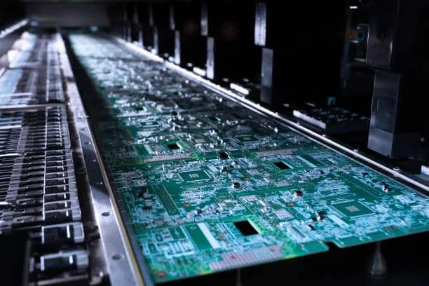
Professional fabrication of double layer HF PCB may include:
-
Tight dielectric thickness control
-
Accurate copper roughness management
-
Controlled impedance verification
-
RF material lamination expertise
-
Precision etching for fine RF traces
Process consistency is essential to maintain stable RF performance across batches.
Conclusion
Double Layer HF PCB provides an efficient and reliable solution for RF and microwave applications requiring stable impedance and low signal loss. By combining proper material selection, accurate impedance control, and optimized grounding design, two-layer high frequency PCBs deliver excellent performance while maintaining cost efficiency.
For RF modules, antennas, and wireless systems, double layer HF PCB remains a practical and effective choice.
