What Is a Fine Pitch PCB?
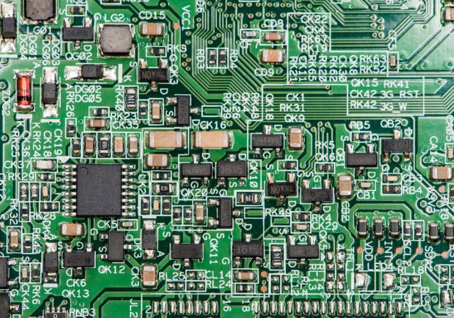
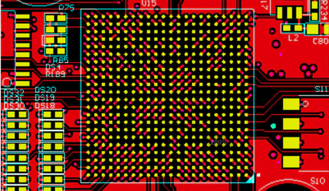
A Fine Pitch PCB is a printed circuit board designed to support fine-pitch components, such as fine-pitch BGA, QFN, CSP, and high pin count ICs, where the spacing between pads and traces is extremely small. Fine pitch PCB technology is essential for modern electronics that demand high density, compact size, and high electrical performance.
Fine pitch PCBs are widely used in semiconductor testing, high-speed communications, automotive electronics, and advanced industrial systems.
Why Fine Pitch PCB Technology Matters
As IC packages continue to evolve toward smaller pitches and higher pin counts, traditional PCB processes can no longer meet routing and assembly requirements. Fine pitch PCB technology addresses challenges such as:
-
Extremely tight pad and trace spacing
-
High pin count IC fan-out
-
Limited board area with increased functionality
-
Signal integrity at high speeds
-
Assembly reliability for miniature components
Fine pitch PCBs enable designers to integrate complex circuits into compact layouts without compromising performance.
Key Features of Fine Pitch PCBs
A high-quality fine pitch PCB typically includes:
-
Ultra-fine line and space routing
-
High registration accuracy
-
Microvias and HDI structures
-
Controlled impedance traces
-
Optimized solder mask definition
These features ensure accurate routing and stable electrical performance in dense designs.
Fine Pitch PCB Design Considerations
Designing a fine pitch PCB requires close coordination between design and manufacturing. Key considerations include:
-
Pad geometry and solder mask opening control
-
Via-in-pad and microvia fan-out strategies
-
Stackup optimization for high-speed signals
-
Crosstalk and EMI suppression
-
Manufacturability and assembly yield
Proper design rules significantly improve reliability and production efficiency.
Materials Used in Fine Pitch PCBs
Material selection plays a critical role in fine pitch PCB performance. Common options include:
-
High-Tg FR-4 for dense digital designs
-
Low-loss laminates for high-speed and RF applications
-
Hybrid material stackups for mixed-signal boards
-
High-reliability materials for automotive and industrial use
Choosing the right materials ensures electrical stability and long-term durability.
Manufacturing Capabilities for Fine Pitch PCBs
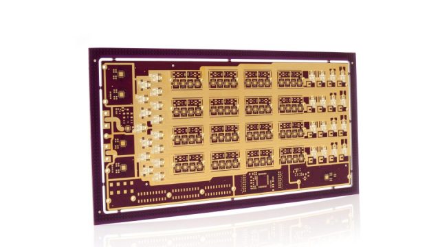
Fine pitch PCB manufacturing requires advanced fabrication processes, including:
-
HDI PCB technology
-
Laser-drilled microvias
-
Advanced imaging and etching
-
Tight layer-to-layer registration
-
AOI and electrical testing
Strict process control is essential to achieve consistent quality.
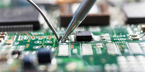
Assembly Challenges of Fine Pitch PCBs
Fine pitch PCB assembly often involves:
-
Fine-pitch BGA and CSP soldering
-
Precise solder paste printing
-
Optimized reflow profiles
-
X-ray inspection for hidden solder joints
-
High-accuracy placement equipment
Professional assembly ensures reliable interconnections for fine-pitch components.
Applications of Fine Pitch PCBs
Fine pitch PCBs are widely used in:
-
Semiconductor test boards and ATE systems
-
IC test PCBs and load boards
-
High-speed computing and networking equipment
-
5G and RF communication modules
-
Automotive electronics and ADAS systems
-
Medical and industrial electronics
They are essential wherever compact design and high performance are required.
Why Choose a Professional Fine Pitch PCB Manufacturer
An experienced fine pitch PCB manufacturer offers:
-
Deep HDI and fine-line process expertise
-
Support for high pin count ICs
-
Stable quality for complex layouts
-
Fast prototype and small-batch production
-
One-stop PCB fabrication and assembly services
The right manufacturing partner helps reduce risk and shorten development cycles.
