
Engineering Context
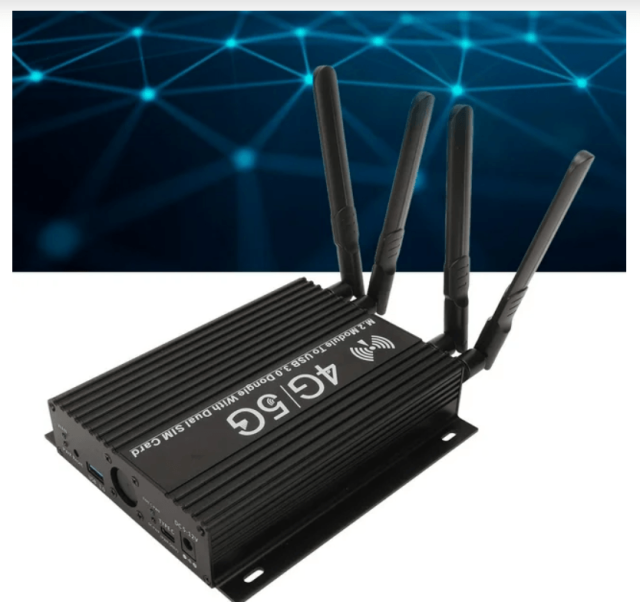
5G router systems represent the backbone of next-generation wireless communication infrastructure, enabling ultra-high-speed data transmission, low-latency connectivity, and massive device interconnection. At the PCB level, these systems require precise RF engineering to ensure stable signal routing between modem chips, RF front-end modules, power amplifiers, and high-speed digital processors.
A 5G Router PCB must simultaneously handle multiple frequency domains, including sub-6 GHz RF communication, mmWave signal processing, and multi-gigabit digital interfaces such as PCIe, Ethernet, and high-speed memory buses. As a result, signal integrity, impedance consistency, and EMI control become critical design constraints.
Unlike conventional networking PCBs, 5G router boards operate in hybrid environments where RF and high-speed digital signals coexist within tightly constrained multilayer stackups. Even minor variations in dielectric constant or trace geometry can introduce reflection, phase distortion, or insertion loss, degrading overall system throughput.
KKCPB designs 5G Router PCBs using RF simulation-driven stackups, controlled impedance routing, and low-loss material selection to ensure stable high-frequency performance across all communication channels.
Core Engineering Challenges
| Engineering Challenge | Root Cause | System Impact |
|---|---|---|
| Signal attenuation at high frequency | Dielectric loss and copper roughness | Reduced data throughput |
| Impedance mismatch in RF paths | Stackup inconsistency | Reflection and return loss |
| EMI coupling between RF and digital sections | Dense routing and poor isolation | Packet errors and jitter |
| Phase instability in RF chains | Material variation and thermal drift | Reduced beamforming accuracy |
| Crosstalk in high-speed interfaces | Insufficient spacing and grounding | Data corruption and latency |
These challenges are amplified in 5G routers due to the simultaneous processing of RF, microwave, and high-speed digital signals on a single PCB platform.
Material Science & RF Performance Requirements
5G Router PCBs rely on advanced materials that can support both RF transmission and high-speed digital routing.
Key Electrical Requirements
| Parameter | Engineering Target | Benefit |
|---|---|---|
| Low Dielectric Constant (Dk) | Stable across GHz range | Impedance consistency |
| Low Dissipation Factor (Df) | Minimal signal loss | High RF efficiency |
| Thermal Stability | High Tg materials | Reduced phase drift |
| Low Copper Roughness | Smooth signal paths | Lower insertion loss |
| Moisture Resistance | <0.1% absorption | Long-term reliability |
Common materials include Rogers RO4003C, RO4350B, RO3003, and high-performance low-loss laminates for RF layers, combined with high-Tg FR-4 or Megtron-type materials for digital sections.
KKCPB Case Study — 5G Router High-Speed RF PCB Platform
Client & Application Context
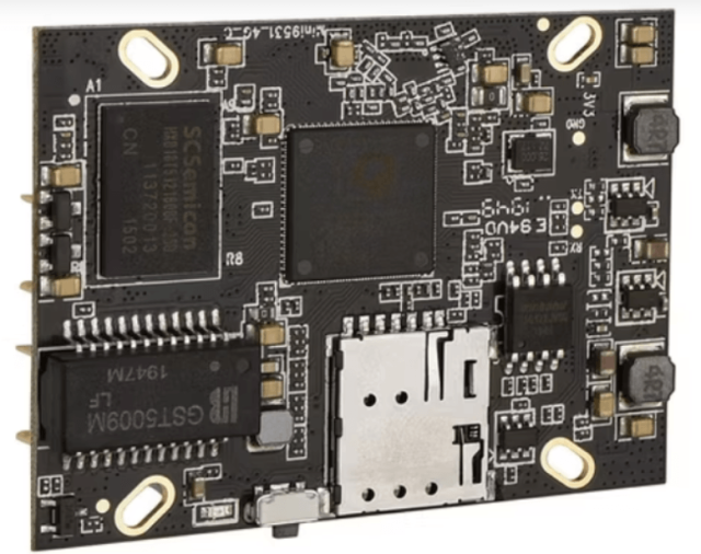
A global networking equipment manufacturer required a high-performance 5G router PCB for enterprise-grade wireless communication systems supporting:
- 5G sub-6 GHz RF transceiver modules
- High-speed 10GbE / 25GbE Ethernet interfaces
- PCIe-based modem integration
- Multi-band antenna control system
- Embedded AI network optimization processor
The system required stable RF performance and ultra-low latency data routing.
Engineering Problem
The initial PCB design exhibited multiple system-level issues:
- RF insertion loss up to 0.48 dB/in at 3.5 GHz
- Impedance deviation of ±6.8% in RF routing layers
- Severe EMI coupling between RF front-end and digital CPU section
- Packet jitter in high-speed Ethernet lanes
- Thermal drift affecting RF calibration stability
These issues resulted in unstable throughput and inconsistent 5G connectivity performance under load conditions.
KKCPB Engineering Solution
KKCPB implemented a hybrid RF + high-speed digital PCB architecture:
- RF signal layers upgraded to low-loss microwave laminate
- Controlled impedance routing with ±2% tolerance design target
- Strategic ground segmentation between RF and digital domains
- Via stitching to improve EMI shielding effectiveness
- Length matching optimization for high-speed differential pairs
- Power integrity optimization using multi-layer decoupling network
- Thermal balancing across RF transceiver zones
Measured Results
| Parameter | Baseline Design | KKCPB Optimized PCB |
|---|---|---|
| RF Insertion Loss @ 3.5 GHz | 0.48 dB/in | 0.22 dB/in |
| Impedance Variation | ±6.8% | ±1.9% |
| EMI Coupling | High | Reduced by 36% |
| Ethernet Jitter | High | Stable within spec |
| RF Phase Drift | Noticeable | <0.5° |
| System Throughput Stability | Fluctuating | Highly stable |
Outcome
The optimized 5G Router PCB significantly improved overall system performance, enabling stable high-speed wireless connectivity and improved multi-device handling capability. RF performance improvements reduced signal degradation, while improved EMI control enhanced coexistence between RF and digital subsystems.
From a procurement and system integration perspective, the improved yield and reduced calibration requirements significantly lowered production and maintenance costs.
Stackup Design & RF Implementation
Hybrid 10-Layer 5G Router PCB Stackup
| Layer | Function | Material |
|---|---|---|
| L1 | RF Signal Layer | Low-loss RF laminate |
| L2 | Ground Plane | Copper |
| L3 | High-speed Digital | High-Tg material |
| L4 | Power Distribution | High-Tg material |
| L5 | RF Control Layer | RF laminate |
| L6 | Ground Plane | Copper |
| L7 | High-speed Interface | High-Tg material |
| L8 | Power Plane | High-Tg material |
| L9 | RF Secondary Layer | RF laminate |
| L10 | Mechanical Support | High-Tg FR-4 |
Simulation & Validation
HFSS EM Simulation
- RF antenna feed optimization
- EMI coupling suppression modeling
ADS RF Circuit Simulation
- S-parameter tuning
- Insertion loss optimization
TDR Analysis
- Impedance discontinuity detection
- Differential pair validation
Thermal FEM Simulation
- RF module thermal drift analysis
- Power density distribution optimization
Environmental & Reliability Validation
| Test | Condition | Result |
|---|---|---|
| Thermal Cycling | -40°C to +85°C | Stable RF performance |
| Humidity Test | 85°C / 85% RH | No dielectric drift |
| Vibration Test | 5–500 Hz, 10G | No structural failure |
| Solder Reflow | 260°C ×3 cycles | No warpage >0.1 mm |
| Long-Term RF Load | Continuous operation | Stable insertion loss |
| EMI Compliance Test | Full system scan | Passed with margin |
Engineering Summary & Contact
5G Router PCBs are foundational to modern wireless communication infrastructure, requiring tight integration of RF, microwave, and high-speed digital design principles. Achieving stable performance demands precise control of impedance, material selection, EMI isolation, and thermal behavior across multilayer stackups.
KKCPB delivers advanced 5G Router PCB engineering solutions combining low-loss RF materials, controlled impedance design, and full-system simulation validation. These capabilities ensure high-speed data transmission, stable RF performance, and reliable operation in complex communication environments.
For 5G router PCB design, RF stackup engineering, and high-speed communication system development, contact KKCPB Engineering Team for customized manufacturing and optimization support.
