As wireless communication, high-speed connectivity, and microwave electronics continue to advance, engineers face increasing challenges in maintaining stable signal transmission at GHz frequencies. In applications such as 5G base stations, RF front-end modules, radar sensing, satellite communication, and antenna systems, the PCB is no longer just a mechanical carrier—it becomes a key part of the RF performance.
Standard FR-4 materials may work well for low-speed digital designs, but they often introduce excessive dielectric loss and unstable impedance at high frequencies. To achieve lower insertion loss and better signal integrity, many high-performance RF designs rely on PTFE PCB materials.
A PTFE PCB is a high frequency printed circuit board manufactured using polytetrafluoroethylene (PTFE) based laminates. Known for ultra-low dielectric loss, stable dielectric constant, and excellent high frequency performance, PTFE PCB is widely used in RF and microwave circuit boards where signal quality and reliability are critical.
What Is a PTFE PCB?
A PTFE PCB is a printed circuit board fabricated with PTFE-based dielectric materials. PTFE is widely used in high-frequency PCB manufacturing due to its electrical properties, especially for microwave signal transmission and controlled impedance routing.
Compared to standard FR-4, PTFE PCB provides:
-
Ultra-low dielectric loss for reduced insertion loss
-
Stable dielectric constant (Dk) for predictable impedance control
-
Better performance for high frequency signal transmission
-
Improved signal integrity for RF traces and microwave circuits
-
High reliability for demanding RF applications
Many well-known high frequency materials are PTFE-based, including various Rogers and Duroid laminates used in advanced RF and microwave PCBs.
Why PTFE PCB Is Used in High Frequency and RF Designs
1. Ultra-Low Loss for High Frequency Signal Transmission
At GHz frequencies, dielectric loss becomes one of the main causes of signal attenuation. PTFE PCB materials are designed to reduce loss and help maintain strong RF signal strength.
PTFE PCB low-loss performance supports:
-
Lower insertion loss for long RF trace routing
-
Improved RF efficiency and link budget
-
Better performance for microwave filters and couplers
-
Stable signal transmission for high frequency signal PCB designs
For high frequency and microwave applications, PTFE PCB is often selected when low loss is a key requirement.
2. Stable Dielectric Properties for Controlled Impedance PCB Routing
Controlled impedance is critical for RF PCB and microwave PCB designs. If dielectric properties vary, impedance can shift and cause reflections, return loss issues, and degraded performance.
PTFE PCB materials help achieve:
-
Consistent microstrip and stripline impedance
-
Stable return loss and reduced signal reflection
-
Predictable RF performance across temperature ranges
-
Repeatable impedance results across production batches
This makes PTFE PCB a reliable choice for controlled impedance PCB manufacturing.
3. Excellent Signal Integrity for RF Trace PCB Layouts
Signal integrity is essential in high frequency circuits. PTFE PCB reduces dielectric loss and supports cleaner waveforms with less distortion.
PTFE PCB signal integrity advantages include:
-
Reduced attenuation and waveform degradation
-
Lower noise coupling and improved RF performance
-
Better consistency in high frequency transmission lines
-
Improved stability for sensitive RF front-end modules
When designing RF trace PCB structures such as microstrip and stripline, PTFE PCB materials provide a strong foundation for stable performance.
Common Applications of PTFE PCB
PTFE PCB is widely used in industries where high frequency performance and reliability are required:
-
5G wireless communication infrastructure
-
RF front-end modules and high frequency amplifiers
-
Radar systems and automotive radar sensors
-
Satellite communication equipment
-
Antenna feed networks and antenna matching circuits
-
Microwave filters, couplers, and power dividers
-
Aerospace and defense RF electronics
-
High frequency test and measurement equipment
If your design includes GHz-level signals, PTFE PCB is often a recommended material option.
PTFE PCB vs FR-4 PCB: Key Differences
FR-4 is a general-purpose PCB material widely used in consumer and industrial electronics. However, at high frequencies, FR-4 limitations become more visible.
FR-4 Challenges at High Frequency
-
Higher insertion loss at GHz frequencies
-
Less stable dielectric constant (Dk)
-
Increased impedance variation and reflections
-
Reduced signal integrity and higher attenuation
PTFE PCB Advantages
-
Much lower dielectric loss and improved signal transmission
-
Stable impedance control for RF traces
-
Better performance for microwave and high frequency circuits
-
More suitable for high reliability RF systems
For RF and microwave designs, PTFE PCB is often chosen to achieve stable performance and meet strict loss budgets.
PTFE PCB Design Considerations
To achieve the best performance from PTFE PCB, engineers should focus on proper high frequency design practices:
1. Stack-Up Planning
Stack-up directly impacts controlled impedance and loss performance. PTFE PCB stack-up design should include stable reference planes and optimized dielectric thickness.
2. Microstrip and Stripline Routing
PTFE PCB supports both microstrip and stripline routing structures. Microstrip is often used for RF trace PCB layouts on outer layers, while stripline is preferred for EMI-sensitive multilayer designs.
3. Via Transitions and RF Discontinuities
Vias can introduce impedance discontinuities. For PTFE PCB designs, optimizing via transitions helps reduce reflections and improve return loss.
4. Grounding and EMI Control
High frequency circuits require strong grounding strategies. Via stitching, continuous ground planes, and proper return path control help improve PTFE PCB performance.
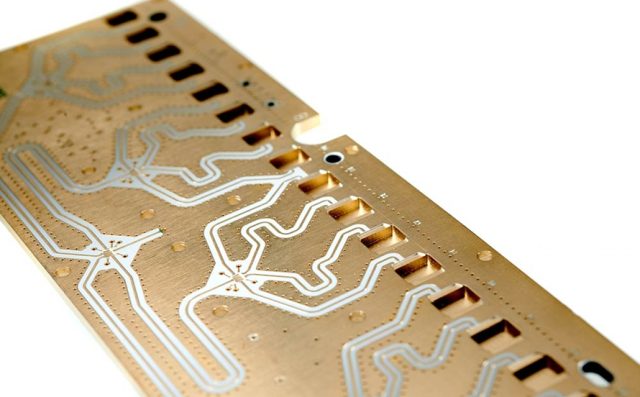
PTFE PCB Manufacturing Considerations
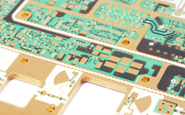
PTFE PCB fabrication requires specialized manufacturing capability because PTFE materials behave differently from standard FR-4.
Key PTFE PCB manufacturing requirements include:
-
Precise lamination control for consistent dielectric thickness
-
Accurate etching for controlled impedance trace geometry
-
Reliable drilling and via plating for multilayer builds
-
Stable process control for repeatable RF performance
-
Controlled impedance testing when required
Working with an experienced PTFE PCB manufacturer helps ensure your RF and microwave circuit boards meet performance expectations.
Conclusion: PTFE PCB for High Frequency and Microwave Circuit Boards
A PTFE PCB is an ideal solution for RF and microwave applications requiring ultra-low loss, stable dielectric properties, and reliable controlled impedance performance. From 5G infrastructure and radar systems to satellite communication and antenna designs, PTFE PCB materials enable high frequency signal transmission with improved signal integrity and reduced insertion loss.
If you are developing high frequency products and need PTFE PCB fabrication, controlled impedance PCB manufacturing, or high reliability RF PCB production, KKPCB can support your project from stack-up review to mass production.
