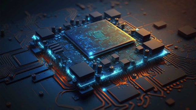
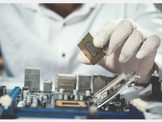
A High Speed IC Test PCB is a specialized semiconductor test PCB designed for high-frequency and high-speed integrated circuits. These boards are critical for processor, memory, RF, and communication IC testing, where signal integrity and timing accuracy are essential.
High-speed ICs operate at frequencies where even minor impedance mismatches, crosstalk, or signal reflections can significantly affect test results. Therefore, the design and fabrication of high-speed IC test PCBs must focus on controlled impedance, low-loss materials, and precise routing.
Key Design Considerations for High Speed IC Test PCBs
1. Controlled Impedance and Signal Integrity
High-speed signals require precise impedance control, trace length matching, and optimized return paths to prevent reflections, crosstalk, and timing errors during testing.
2. Low-Loss PCB Materials
Using low dielectric loss materials such as RO4003, FR408HR, or PTFE-based laminates reduces signal attenuation and preserves high-frequency integrity.
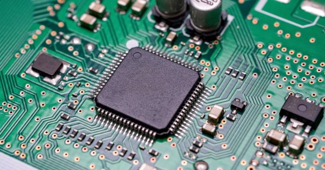
3. High Pin Count and HDI Routing
Modern ICs often have hundreds of pins, necessitating HDI technology, microvias, fine-line routing, and multilayer stackups to ensure reliable connections.
4. Robust Power Distribution
A carefully designed power distribution network (PDN) with low-impedance planes and decoupling minimizes voltage fluctuations and noise that could affect high-speed measurements.
5. Thermal and Mechanical Stability
High-speed IC test boards must maintain dimensional stability and flatness under thermal and mechanical stress to ensure repeatable and reliable contact with test sockets or probes.
Applications of High Speed IC Test PCBs
High speed IC test PCBs are widely used in:
-
High-performance processor testing
-
DDR and high-speed memory IC validation
-
High-frequency communication IC testing (5G, RF front-end, mmWave)
-
Automotive ADAS and infotainment IC testing
-
Industrial high-speed IC qualification
These applications demand accurate timing, low signal loss, and repeatable results.
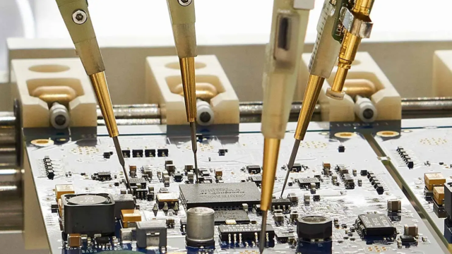
Manufacturing Requirements for High Speed IC Test PCBs
High-quality high-speed IC test PCBs require:
-
Multilayer HDI PCB fabrication
-
Microvia drilling and fine-line etching
-
Controlled impedance verification
-
Low-loss material lamination
-
Prototype, small batch, and volume production support
Strict process control ensures consistent electrical performance and reliable high-speed testing.
Why High Speed IC Test PCB Quality Matters
Low-quality boards can cause:
-
Signal integrity issues and timing errors
-
Inaccurate or inconsistent test results
-
Increased debugging cycles and lower test yield
-
Higher operational and production costs
A professionally designed High Speed IC Test PCB guarantees accurate validation, reliable ATE testing, and optimal test efficiency.
Conclusion
The High Speed IC Test PCB is a critical tool for validating high-frequency and high-speed ICs, ensuring reliable performance in demanding test environments. Through controlled impedance, low-loss materials, HDI routing, and robust power design, these boards deliver high-precision, repeatable testing.
Partnering with an experienced high-speed IC test PCB manufacturer ensures faster validation, improved yield, and long-term reliability for high-performance semiconductor applications.
