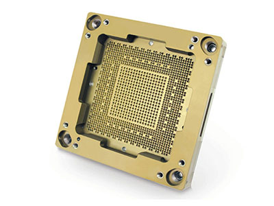
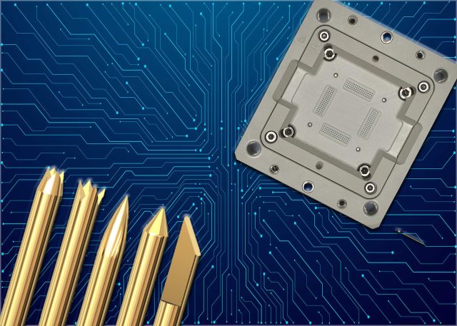
A Test Socket PCB for IC is a specialized semiconductor test PCB designed to mount and support IC test sockets, forming a critical interface between the integrated circuit under test and Automated Test Equipment (ATE). These PCBs play a key role in ensuring stable signal transmission, reliable mechanical alignment, and repeatable test results throughout IC validation and production testing.
As IC packages evolve toward higher pin counts, finer pitches, and higher operating speeds, test socket PCBs must meet increasingly strict requirements for signal integrity, mechanical accuracy, and durability.
Key Design Requirements for Test Socket PCBs
1. High Pin Count and Fine-Pitch Support
Modern IC test sockets often accommodate packages with hundreds or thousands of pins, requiring high-density routing, HDI technology, and multilayer PCB structures to ensure reliable signal access.
2. Controlled Impedance and Signal Integrity
High-speed and high-frequency ICs demand precise controlled impedance routing, short signal paths, and length matching to minimize reflections, crosstalk, and signal loss during testing.
3. Mechanical Accuracy and Flatness
Test socket PCBs must maintain excellent flatness and dimensional stability to ensure consistent contact between the socket pins and the IC under repeated insertion and removal cycles.
4. Robust Power and Ground Design
A stable power distribution network (PDN) with optimized ground planes and decoupling capacitors ensures consistent voltage delivery and reduces noise during sensitive IC measurements.
5. Durability for Repeated Test Cycles
High-quality materials and precise manufacturing allow test socket PCBs to withstand frequent socket mounting, thermal cycling, and long test durations without degradation.
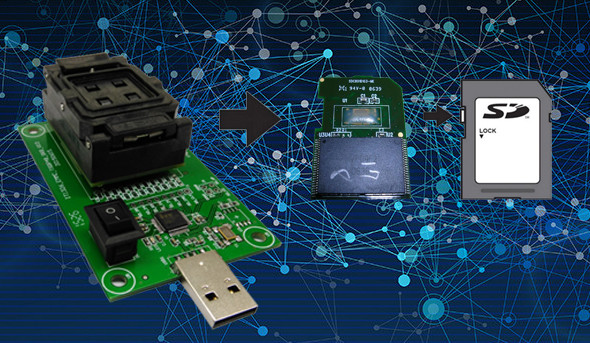
Applications of Test Socket PCBs for ICs
Test socket PCBs are widely used in:
-
Logic and processor IC testing
-
Memory IC validation
-
RF and mixed-signal IC testing
-
Automotive and industrial IC qualification
-
High-speed interface and communication IC testing
These applications require repeatable electrical performance and reliable mechanical interfaces.
Manufacturing Considerations for Test Socket PCBs
Producing high-quality Test Socket PCBs for ICs requires advanced PCB manufacturing capabilities, including:
-
Multilayer and HDI PCB fabrication
-
Fine-line etching and microvia processing
-
Controlled impedance testing and verification
-
Tight mechanical tolerance and flatness control
-
Support for prototype, small batch, and volume production
Precise manufacturing ensures consistent performance across multiple test boards and test environments.
Why Test Socket PCB Quality Matters
Low-quality test socket PCBs can result in:
-
Intermittent electrical contact and unstable signals
-
Measurement errors and inconsistent test results
-
Increased socket wear and equipment downtime
-
Reduced test yield and higher operational costs
A professionally engineered Test Socket PCB for IC ensures accurate, repeatable testing, improved reliability, and longer socket lifespan.
Conclusion
The Test Socket PCB for IC is a vital component in modern semiconductor testing, providing a reliable interface between ICs and ATE systems. With high pin count support, controlled impedance routing, robust power design, and mechanical precision, these PCBs enable accurate and repeatable IC validation across a wide range of applications.
Choosing an experienced semiconductor test PCB manufacturer ensures high-quality test socket PCBs that support faster validation cycles, higher yield, and long-term testing reliability.
