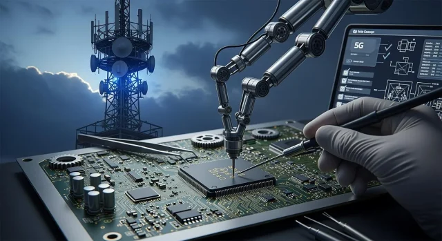
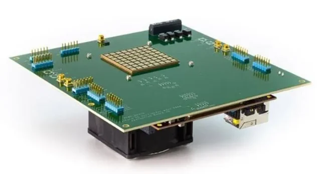
A 5G IC Test PCB is a specialized semiconductor test PCB engineered to validate high-speed 5G ICs used in RF front-end modules, baseband processors, mmWave transceivers, and 5G communication devices. With the rapid adoption of 5G technology, ICs operate at higher frequencies, faster data rates, and compact packages, making precise PCB design essential for accurate functional, parametric, and performance testing.
These boards act as the interface between the IC under test and Automated Test Equipment (ATE), ensuring stable connections, signal integrity, and repeatable measurements during rigorous testing cycles.
Key Features of 5G IC Test PCBs
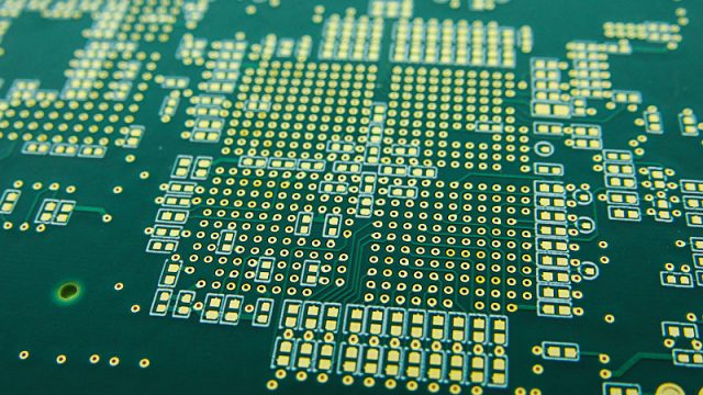
1. Controlled Impedance and Signal Integrity
High-speed 5G ICs require carefully controlled trace impedance, matched trace lengths, and optimized routing to prevent signal reflection, crosstalk, and distortion.
2. Low-Loss High-Frequency Materials
Substrates like Rogers, Taconic RF-35, or Duroid 5880 reduce insertion loss and maintain stable electrical performance at mmWave frequencies, ensuring accurate measurement.
3. High Pin Count and Fine-Pitch Routing
5G ICs often feature hundreds of pins with fine-pitch packages, requiring HDI technology, microvias, and multilayer PCB stackups to maintain reliable connectivity.
4. Thermal and Mechanical Stability
Materials with high Tg and dimensional stability enable the PCB to endure extended testing cycles and thermal stress without compromising contact reliability.
5. Noise Suppression and Grounding Design
Proper ground plane configuration and signal isolation reduce electromagnetic interference, maintaining accurate measurement for sensitive analog and high-speed digital signals.
Applications of 5G IC Test PCBs
-
mmWave IC testing for RF front-end modules
-
Baseband processor evaluation
-
5G transceiver and module testing
-
Automotive 5G IC verification
-
High-speed communication IC functional and parametric testing
These applications demand high signal fidelity, repeatable results, and low-loss routing.
Manufacturing Considerations for 5G IC Test PCBs
Producing reliable 5G IC test PCBs requires:
-
Multilayer HDI PCB fabrication
-
Fine-line etching and microvia processing
-
Controlled impedance testing and verification
-
Low-loss material selection
-
Prototype, small batch, and volume production support
Advanced manufacturing ensures stable electrical performance, high-frequency reliability, and accurate test results.
Why High-Quality 5G IC Test PCBs Matter

Poorly designed PCBs can cause:
-
Signal degradation and measurement errors
-
Unstable test connections and repeatability issues
-
Increased test failures and debugging time
-
Reduced production yield and higher costs
