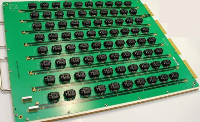
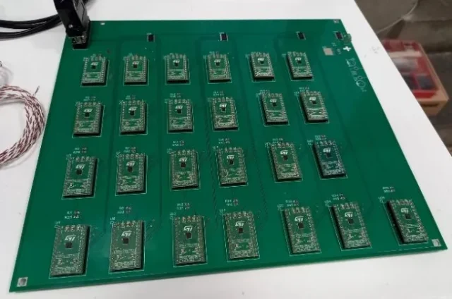
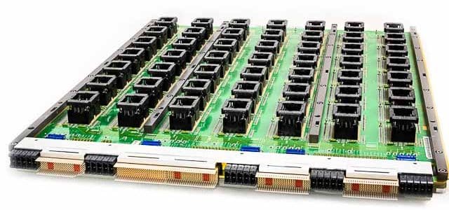
A Burn-in Board PCB is a specialized semiconductor test PCB used in burn-in testing, a process that subjects ICs to elevated temperatures and electrical stress to identify early-life failures and ensure long-term reliability. These boards provide the mechanical and electrical interface between Automated Test Equipment (ATE) and ICs, ensuring precise signal routing and stable power delivery during extended test cycles.
As ICs become faster, denser, and more complex, burn-in board PCBs must meet strict requirements for signal integrity, mechanical precision, thermal stability, and reliability.
Key Design Features of Burn-in Board PCBs
1. High Pin Count and Dense Routing
Burn-in boards often accommodate ICs with hundreds to thousands of pins, requiring HDI technology, fine-line routing, and multilayer stackups for reliable connectivity and accurate signal transmission.
2. Controlled Impedance and Signal Integrity
Accurate testing demands precise controlled impedance, trace length matching, and minimized crosstalk, ensuring reliable measurement of IC performance even under thermal stress.
3. Mechanical Accuracy and Reliability
Burn-in PCBs must maintain flatness, dimensional stability, and pad alignment to ensure consistent contact with sockets or test fixtures over prolonged stress testing cycles.
4. Robust Power and Ground Design
Optimized power distribution networks, low-impedance grounds, and decoupling strategies ensure stable voltage supply to ICs, reducing noise and voltage fluctuation during high-temperature burn-in tests.
5. Thermal Stability and Material Selection
High-Tg, low-loss laminates enable burn-in boards to withstand elevated temperatures and prolonged testing durations, ensuring consistent electrical and mechanical performance.
Applications of Burn-in Board PCBs
Burn-in board PCBs are widely used in:
-
Memory IC stress testing
-
Processor and logic IC burn-in validation
-
Mixed-signal and RF IC reliability evaluation
-
Automotive and high-reliability IC qualification
-
High-temperature, high-voltage semiconductor testing
These applications require stable, repeatable, and reliable electrical performance during extended testing periods.
Manufacturing Requirements for Burn-in Board PCBs
Producing high-quality burn-in PCBs requires:
-
Multilayer and HDI PCB fabrication
-
Fine-line etching and microvia technology
-
Controlled impedance verification
-
High pin count and tight tolerance processing
-
Thermal-resistant material selection for extended stress testing
-
Prototype, small batch, and volume production support
Advanced manufacturing ensures consistent electrical performance, mechanical stability, and reliable burn-in results.
Why Burn-in Board PCB Quality Matters
Inferior burn-in boards can lead to:
-
Inconsistent IC contact and unreliable signals
-
Measurement errors and false failures
-
Increased test equipment downtime
-
Reduced test yield and higher operational costs
High-quality Burn-in Board PCBs guarantee accurate, repeatable, and reliable stress testing, ensuring IC reliability and long-term performance.
Conclusion
The Burn-in Board PCB is a crucial component for semiconductor reliability testing, providing precise electrical routing, controlled impedance, and thermal stability for extended IC stress tests. With advanced HDI design, multilayer construction, and premium materials, burn-in PCBs enable accurate, repeatable, and reliable testing for modern ICs.
Partnering with a professional burn-in board PCB manufacturer ensures high test accuracy, improved IC yield, and long-term reliability in demanding ATE burn-in environments.
