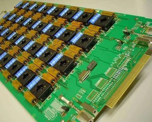
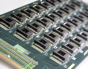
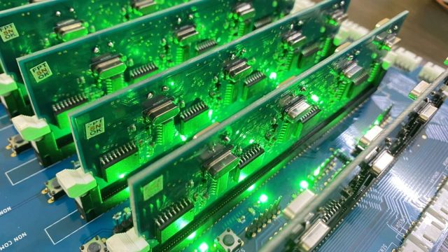
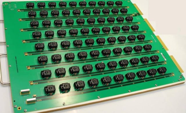
A Burn-in Board PCB is a specialized semiconductor test PCB designed to support burn-in testing, a process that subjects ICs and semiconductor devices to elevated temperatures and voltage stresses to detect early-life failures. These PCBs are critical in Automated Test Equipment (ATE) systems, providing a reliable interface between the test setup and the device under test (DUT) while maintaining signal integrity, power stability, and mechanical reliability.
As ICs advance toward higher pin counts, smaller package sizes, and higher-speed operation, burn-in board PCBs must deliver precise electrical performance and robust mechanical design to ensure accurate stress testing.
Key Design Requirements of Burn-in Board PCBs
1. High Pin Count and Dense Routing
Burn-in boards often support ICs with hundreds to thousands of I/O pins, including BGA, LGA, QFN, and CSP packages. HDI routing, fine-line traces, and multilayer stackups are critical for reliable high-density interconnections.
2. Controlled Impedance and Signal Integrity
High-speed and mixed-signal ICs require precise impedance control, trace length matching, and crosstalk suppression to ensure accurate voltage and signal application during burn-in tests.
3. Thermal Management and Material Selection
Burn-in testing involves elevated temperatures. High-Tg and low-loss laminates, along with robust thermal design, ensure that the PCB maintains mechanical stability and electrical performance under prolonged stress.
4. Power Integrity and Noise Reduction
Stable power delivery across all pins is essential for accurate stress testing. Optimized power and ground planes, decoupling strategies, and low-impedance PDN design reduce voltage fluctuations and noise during burn-in cycles.
5. Mechanical Durability and Reliability
Repeated insertion, high-temperature cycles, and mechanical handling demand precise PCB tolerances, flatness, and robust mechanical design to maintain reliable connections to sockets and probes.
Applications of Burn-in Board PCBs
Burn-in board PCBs are commonly used in:
-
Memory IC and DRAM testing
-
Logic IC and microprocessor stress validation
-
RF and mixed-signal IC reliability testing
-
Automotive semiconductor burn-in
-
High-reliability IC qualification for aerospace and industrial applications
These applications demand high reliability, precise electrical contact, and stable thermal performance.
Manufacturing Capabilities for Burn-in Board PCBs
Producing high-quality burn-in board PCBs requires:
-
HDI and multilayer PCB fabrication
-
Fine-line etching and microvia technology
-
Controlled impedance verification
-
High-Tg, low-loss material processing
-
Prototype, small batch, and mass production capabilities
Advanced manufacturing ensures that burn-in boards provide consistent electrical and mechanical performance across repeated thermal cycles.
Why Burn-in Board PCB Quality Matters
Low-quality burn-in boards can cause:
-
Unstable IC contact and poor electrical connectivity
-
Signal distortion and voltage drop across high pin counts
-
Reduced reliability and inconsistent test results
-
Increased maintenance, downtime, and IC yield loss
High-quality burn-in board PCBs guarantee accurate, repeatable, and reliable IC stress testing, improving overall semiconductor quality and production yield.
Conclusion
The Burn-in Board PCB is an essential component for semiconductor stress testing, providing high pin count routing, controlled impedance, and mechanical stability. Through precision HDI design, robust materials, and advanced manufacturing, burn-in boards ensure reliable, repeatable, and high-accuracy stress testing for modern ICs.
Partnering with an experienced burn-in board PCB manufacturer ensures improved test accuracy, reduced downtime, and enhanced semiconductor reliability, supporting applications in memory, logic, RF, automotive, and industrial electronics.
