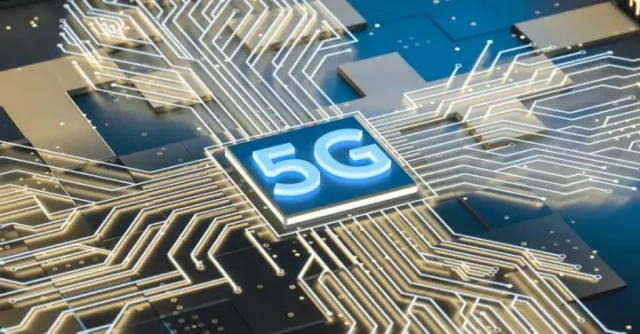
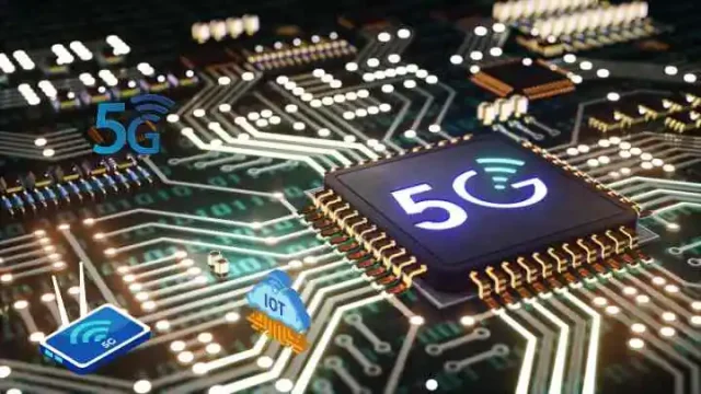
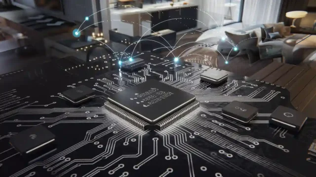
A 5G IC Test PCB is a specialized high-frequency semiconductor test PCB designed to validate 5G-related integrated circuits, including 5G baseband ICs, RF transceivers, power amplifiers, and mmWave front-end modules. Installed in Automated Test Equipment (ATE) systems, the 5G IC test PCB ensures accurate signal transmission, precise impedance control, and reliable power delivery across sub-6 GHz and mmWave frequency bands.
As 5G technology advances toward higher bandwidth, lower latency, and higher integration, the electrical performance requirements for 5G IC test PCBs have become significantly more demanding. Any impedance deviation, dielectric loss, or signal coupling can directly affect test accuracy and yield.
Key Technical Requirements of 5G IC Test PCBs
1. Controlled Impedance for High-Frequency Signals
5G IC testing requires tight impedance control across RF and high-speed digital traces. Optimized stackups and precision trace geometry ensure minimal signal reflection and stable RF performance.
2. Low-Loss RF Materials and Hybrid Stackups
To minimize signal attenuation, low-Dk and low-Df laminates are commonly used. Hybrid stackups combining RF materials and high-Tg FR-4 support both RF and digital domains on the same test board.
3. High-Frequency Signal Integrity and Isolation
Proper ground referencing, shielding structures, and isolation techniques reduce RF leakage, crosstalk, and electromagnetic interference during 5G IC testing.
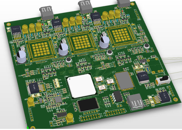
4. High-Density and High Pin Count Design
5G ICs often feature fine-pitch, high I/O packages. HDI PCB technology enables dense routing while maintaining signal and power integrity.
5. Stable Power Integrity for RF Performance
Clean and stable power delivery is critical for RF accuracy. Robust power plane design and decoupling strategies minimize noise and voltage ripple.
Applications of 5G IC Test PCBs
5G IC Test PCBs are widely used in:
-
5G baseband and modem IC testing
-
RF transceiver and power amplifier validation
-
mmWave front-end module testing
-
5G antenna interface and beamforming IC evaluation
-
Automotive and industrial 5G semiconductor testing
These applications demand high-frequency accuracy, repeatability, and long-term reliability.
Manufacturing Capabilities for 5G IC Test PCBs
Producing a reliable 5G IC Test PCB requires advanced manufacturing expertise:
-
Controlled impedance fabrication and RF verification
-
Low-loss RF laminate and hybrid stackup processing
-
HDI and multilayer PCB fabrication (often 12–30+ layers)
-
Precision drilling and fine-line etching
-
Prototype, small batch, and volume production support
These capabilities ensure consistent RF performance across all testing phases.
Why 5G IC Test PCB Quality Matters
Inaccurate RF performance or signal loss in a 5G IC test PCB can lead to measurement errors, reduced yield, and delayed product validation. A high-quality test PCB ensures:
-
Accurate RF and high-speed digital measurements
-
Reduced test uncertainty and calibration effort
-
Improved test throughput and efficiency
-
Reliable performance in high-volume semiconductor testing
Conclusion
The 5G IC Test PCB is a cornerstone of modern 5G semiconductor testing, enabling accurate validation of high-frequency, high-speed, and mmWave ICs. Through controlled impedance routing, low-loss materials, HDI PCB technology, and robust power integrity, 5G IC test PCBs ensure reliable, repeatable, and high-precision testing performance.
Choosing an experienced 5G IC Test PCB manufacturer is essential to achieving
