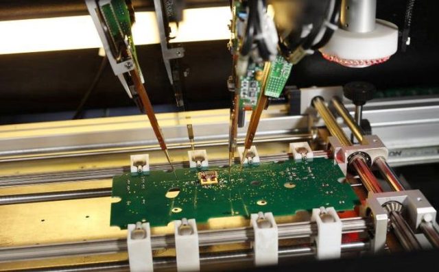
A High Speed IC Test PCB is a specialized semiconductor test PCB designed to validate integrated circuits operating at high data rates and fast edge speeds. These test boards are widely used in Automated Test Equipment (ATE) systems to ensure accurate signal transmission, precise timing measurement, and reliable power delivery during IC characterization and production testing.
As semiconductor devices continue to adopt high-speed interfaces such as DDR, PCIe, SerDes, USB, and high-frequency RF links, the performance requirements for high speed IC test PCBs have increased dramatically. Any impedance mismatch, signal loss, or noise coupling can result in inaccurate measurements and false test failures.
Key Technical Requirements of High Speed IC Test PCBs
1. Controlled Impedance and Signal Integrity
Maintaining tight controlled impedance is essential for high-speed digital and RF signal paths. Carefully engineered stackups and trace geometries minimize reflections, jitter, and timing skew.
2. Low-Loss Materials and Routing
High-speed signals are sensitive to dielectric loss. Low-loss laminates and optimized routing reduce insertion loss and maintain eye diagram integrity.
3. Power Integrity and Decoupling Strategy
High-speed ICs require stable, low-noise power delivery. Robust power distribution networks (PDN), short return paths, and optimized decoupling minimize power-induced jitter.
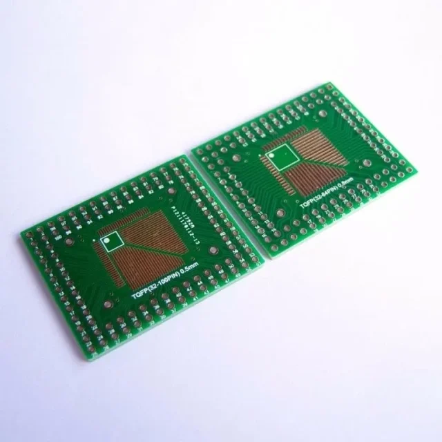
4. High-Density and High Pin Count Design
Advanced high-speed ICs often feature fine-pitch, high I/O packages. HDI PCB technology enables efficient fan-out while preserving signal integrity.
5. Crosstalk and EMI Control
Proper spacing, reference planes, and differential pair routing reduce crosstalk and electromagnetic interference in high speed IC test boards.
Applications of High Speed IC Test PCBs
High Speed IC Test PCBs are used in a wide range of semiconductor test applications, including:
-
High-speed digital IC and processor testing
-
Memory interface validation (DDR, LPDDR, HBM)
-
SerDes and high-speed interface testing
-
RF-enabled and mixed-signal IC validation
-
Automotive, AI, and data center semiconductor testing
These applications demand extreme accuracy and repeatability, making professional PCB design and manufacturing essential.
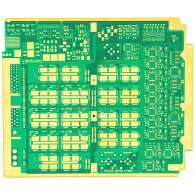
Manufacturing Capabilities for High Speed IC Test PCBs
Producing reliable high speed IC test PCBs requires advanced manufacturing expertise:
-
Controlled impedance fabrication and verification
-
HDI and multilayer PCB construction (often 12–30+ layers)
-
Low-loss and high-Tg laminate processing
-
Precision drilling and fine-line etching
-
Prototype, small batch, and volume production support
These capabilities ensure consistent electrical performance across all test stages.
Why High Speed IC Test PCB Quality Matters
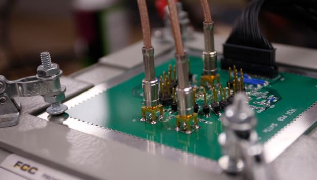
Any signal degradation or power instability in a high speed IC test PCB can lead to measurement errors, reduced yield, and extended debugging cycles. A high-quality board ensures:
-
Accurate timing and signal measurements
-
Reduced test uncertainty and noise coupling
-
Improved test efficiency and throughput
-
Reliable performance in high-volume production environments
Conclusion
The High Speed IC Test PCB is a critical foundation for modern semiconductor testing, enabling accurate validation of today’s fastest and most complex ICs. Through controlled impedance design, low-loss materials, robust power integrity, and HDI PCB technology, high speed IC test PCBs support reliable, repeatable, and high-precision semiconductor testing.
Selecting an experienced high speed IC test PCB manufacturer is essential to achieving consistent test performance and faster time-to-market.
