As data rates continue to rise across semiconductor and electronic systems, high speed test PCBs have become essential for accurate validation and characterization. In automated test equipment (ATE) environments, even minor signal distortion can lead to false failures or inaccurate measurements. A well-designed high speed test PCB ensures reliable signal transmission, precise timing, and repeatable test results.
What Is a High Speed Test PCB?

A high speed test PCB is a specialized printed circuit board designed to support high data rate signals during device validation and testing. It serves as the electrical interface between the device under test (DUT) and test systems, such as ATE or laboratory instruments.
Key functions include:
-
Maintaining signal integrity at multi-gigabit speeds
-
Providing controlled impedance for differential and single-ended signals
-
Minimizing crosstalk, jitter, and insertion loss
-
Supporting high pin count and dense routing requirements
Key Design Challenges in High Speed Test PCBs
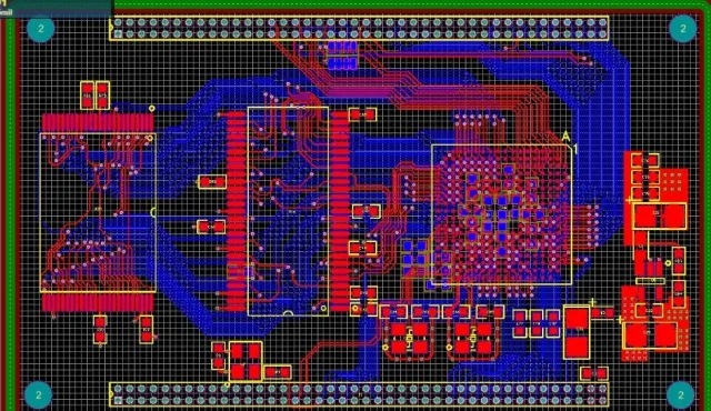
High speed test PCBs must address several technical challenges:
-
Controlled Impedance Routing
Accurate impedance control is critical to prevent reflections and eye diagram closure at high data rates. -
Low-Loss Materials and Stackups
Material selection directly affects insertion loss and signal attenuation in high-speed testing. -
Crosstalk and Noise Control
Careful routing, spacing, and ground referencing are required to reduce noise coupling between adjacent traces. -
Power Integrity
Stable power and ground planes ensure consistent device behavior during high-speed test cycles.
Materials and Stackup Considerations
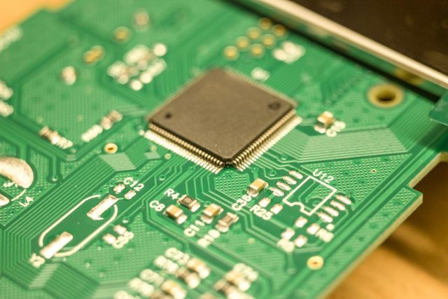
High speed test PCBs often use:
-
High-Tg FR-4 for moderate-speed testing
-
Low-loss laminates for multi-gigabit or high-frequency applications
-
Hybrid stackups combining cost efficiency with electrical performance
Optimized stackup design improves impedance consistency and minimizes signal degradation.
Applications of High Speed Test PCBs
High speed test PCBs are widely used in:
-
Semiconductor IC validation and characterization
-
Wafer test and probe card interfaces
-
Load boards and interface boards for ATE systems
-
High-speed digital and mixed-signal testing
These applications demand precise timing and stable signal integrity.
Selecting a High Speed Test PCB Manufacturer

When choosing a high speed test PCB supplier, consider:
-
Experience with high-speed and high-frequency PCB design
-
Capability for controlled impedance and multilayer fabrication
-
Support for prototype, small batch, and volume production
-
Comprehensive electrical testing and quality control
A reliable manufacturer ensures consistent performance across all testing stages.
Conclusion
High speed test PCBs are critical for accurate validation of modern electronic and semiconductor devices. By combining controlled impedance, low-loss materials, and precise multilayer design, these PCBs enable reliable high-speed testing with minimal signal distortion.
Partnering with an experienced high speed test PCB manufacturer ensures accurate results, faster development cycles, and higher testing confidence.
