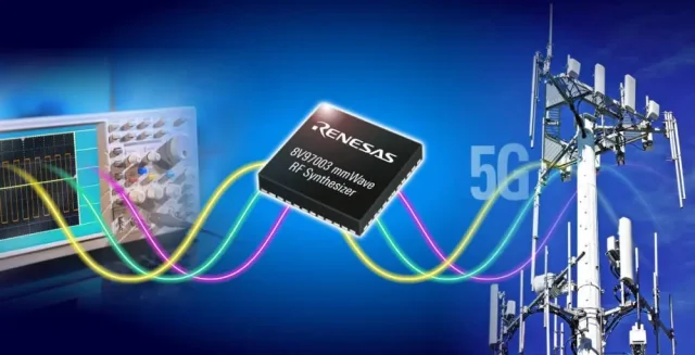
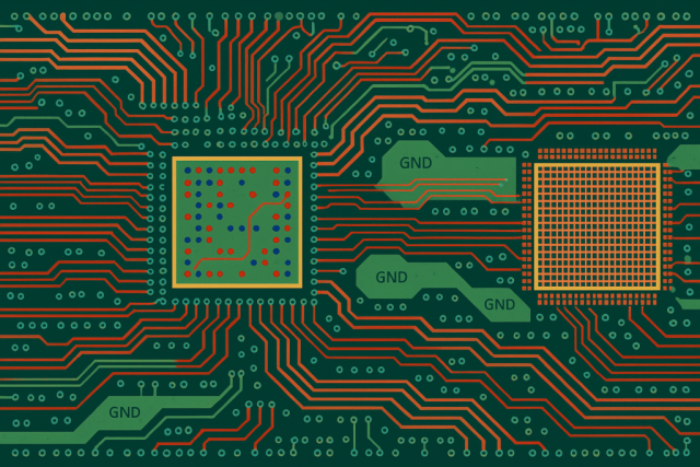
As 5G technology expands into millimeter-wave frequency bands, PCB design enters a new level of complexity. Operating at frequencies above 24 GHz, 5G mmWave PCB designs must manage extreme signal loss sensitivity, tight impedance tolerances, and strict manufacturing precision.
A professionally engineered 5G mmWave PCB is essential for enabling high data rates, low latency, and reliable wireless communication.
What Is a 5G mmWave PCB?
A 5G mmWave PCB is a high-frequency printed circuit board specifically designed to support millimeter-wave signals used in 5G base stations, small cells, antennas, and RF front-end modules.
Unlike conventional RF PCBs, mmWave PCBs operate in frequency ranges where even microscopic layout or material variations can significantly affect performance.
Key Design Challenges in 5G mmWave PCB
Designing a 5G mmWave PCB involves overcoming several critical challenges:
-
Severe dielectric and conductor loss
-
Extremely tight impedance and phase control
-
Sensitivity to surface roughness and copper profile
-
Minimal tolerance for manufacturing variation
Each of these factors must be addressed holistically.
Material Selection for 5G mmWave PCB
Material choice is one of the most critical decisions. Common substrates for 5G mmWave PCB include:
-
Rogers RO4003C for lower mmWave bands
-
Rogers RT/duroid® materials for ultra-low loss paths
-
Taconic RF laminates for antenna and module designs
Low dielectric loss and stable Dk are essential for mmWave performance.
Signal Integrity at Millimeter-Wave Frequencies
At mmWave frequencies, signal integrity is dominated by:
-
Controlled impedance accuracy
-
Trace geometry precision
-
Short, direct signal routing
A 5G mmWave PCB requires tightly controlled transmission line structures to prevent excessive insertion loss and phase distortion.
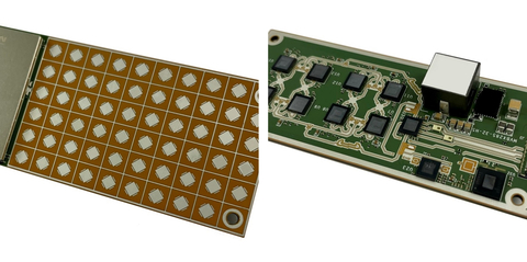
Antenna Integration and RF Front-End Design
Many 5G mmWave PCBs integrate antennas directly onto the PCB. This approach requires:
-
Precise antenna geometry control
-
Consistent dielectric properties
-
Isolation between RF, digital, and power domains
PCB-integrated antennas demand exceptional design and manufacturing alignment.
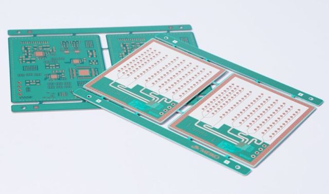
Stackup and Layer Structure Optimization
To support mmWave signals, 5G mmWave PCB stackups are carefully engineered:
-
Thin dielectric layers for impedance accuracy
-
Symmetrical multilayer constructions
-
Dedicated ground reference planes
Stackup imbalance can lead to warpage and performance variation.
Manufacturing Precision and Process Control
Manufacturing a 5G mmWave PCB requires advanced process control:
-
Tight laminate thickness tolerance
-
Smooth copper surface treatments
-
Precise drilling and registration
Even minor deviations can cause significant RF performance shifts at mmWave frequencies.
Testing and Validation of 5G mmWave PCB
Verification of 5G mmWave PCBs includes:
-
Impedance measurement
-
Insertion loss and return loss testing
-
Phase and timing validation
Testing ensures that the PCB meets stringent mmWave performance requirements.
Typical Applications of 5G mmWave PCB
5G mmWave PCBs are widely used in:
-
5G base stations and small cells
-
mmWave antenna arrays
-
RF front-end modules
-
High-speed wireless backhaul systems
Each application requires consistent, repeatable high-frequency performance.
Choosing a 5G mmWave PCB Manufacturing Partner
When selecting a 5G mmWave PCB manufacturer, consider:
-
Proven mmWave PCB experience
-
Capability with low-loss RF materials
-
Controlled impedance and RF testing
-
Support for prototype and volume production
An experienced partner helps reduce development risk and time-to-market.
Conclusion
The 5G mmWave PCB is a critical enabler of next-generation wireless communication. Through precise material selection, signal integrity-driven design, optimized stackup, and controlled manufacturing processes, high-quality mmWave PCBs deliver the performance required for advanced 5G systems.
Working with a specialized 5G mmWave PCB supplier ensures reliable performance from prototype development to mass production.
