Introduction: Why Controlled Impedance Defines High-Speed Reliability
As high-speed electronics push into multi-gigabit data rates and high-frequency RF domains, signal behavior is no longer dominated by logic thresholds—it is governed by transmission line physics. In these systems, every PCB trace behaves as a controlled impedance structure, and any deviation can introduce reflections, timing skew, and electromagnetic interference.
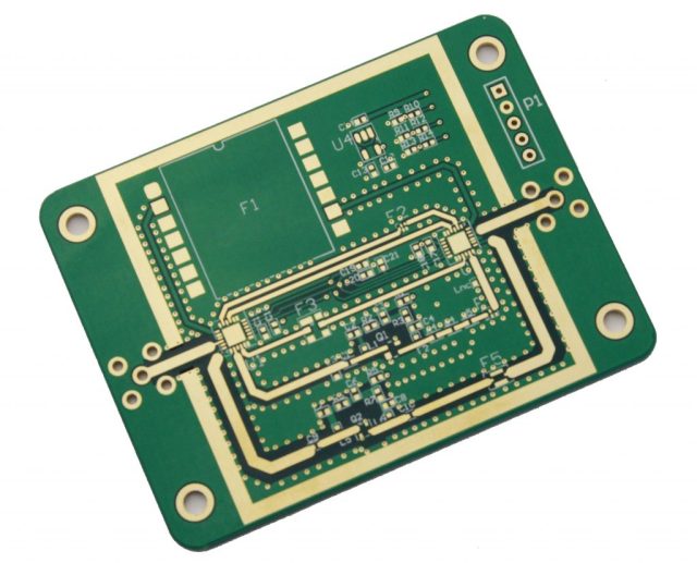
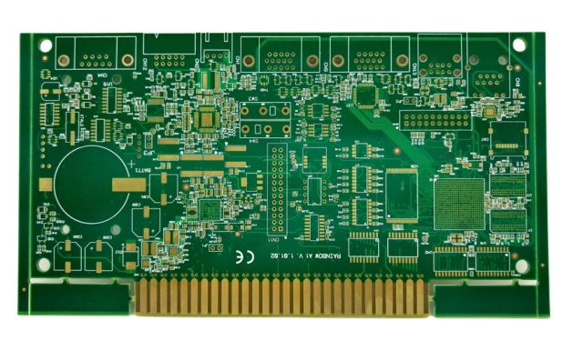
Controlled impedance PCB architectures form the electrical backbone of reliable high-speed electronics. Whether in data center switches, high-speed servers, RF transceivers, automotive ADAS, or satellite communication systems, impedance accuracy directly determines signal integrity, eye margin, and long-term system stability.
Understanding Controlled Impedance in High-Speed PCBs
Controlled impedance refers to maintaining a predictable characteristic impedance along a signal path, typically:
-
50Ω single-ended impedance for RF and clock signals
-
85Ω / 100Ω differential impedance for high-speed serial links
In high-speed PCB designs, impedance is influenced not only by trace width, but by a combination of:
-
Dielectric constant (Dk) of PCB materials
-
Dielectric thickness between signal and reference planes
-
Copper thickness and surface roughness
-
Trace geometry and spacing
-
Via transitions and reference plane continuity
Achieving stable impedance therefore requires a stackup-driven engineering approach, not isolated routing adjustments.
Controlled Impedance PCB Architectures: The Foundation of Signal Integrity
Stackup-Centric Design Strategy
Reliable controlled impedance PCBs start with a properly engineered multilayer stackup. KKPCB adopts a stackup-first methodology that includes:
-
Dedicated reference planes for high-speed signal layers
-
Symmetrical stackups to minimize lamination distortion
-
Optimized signal-to-plane spacing for impedance stability
This approach ensures that impedance targets are inherently achievable during fabrication, not forced through last-minute routing compromises.
Material Selection for Impedance Stability
Material choice is critical for controlled impedance PCBs. KKPCB supports a wide range of high-speed and RF laminates, selected based on:
-
Stable Dk across frequency and temperature
-
Low dissipation factor (Df) to minimize insertion loss
-
Consistent resin flow behavior during lamination
For high-speed digital PCBs, low-loss FR-4 variants and advanced resin systems are commonly used, while RF PCBs may require specialized laminates to ensure impedance consistency at higher frequencies.
Copper Geometry and Process Control
At high frequencies, copper behavior becomes a dominant factor. KKPCB controls impedance variation through:
-
Low-profile or very-low-profile copper foils
-
Etching compensation to maintain designed trace widths
-
Uniform copper plating to prevent post-fabrication impedance drift
These process controls are essential for maintaining tight impedance tolerances across production volumes.
Managing Impedance Discontinuities in Real-World Designs
Via Structures and Transition Optimization
Vias are a major source of impedance discontinuity in high-speed PCBs. KKPCB minimizes their impact using:
-
Backdrilling to eliminate unused via stubs
-
Blind and buried vias to shorten signal transitions
-
Via-in-pad and resin-filled vias for HDI architectures
This is especially critical in high-speed serial channels, RF signal paths, and clock distribution networks.
Reference Plane Integrity and Return Path Control
A controlled impedance PCB is only as good as its return path. KKPCB ensures:
-
Continuous reference planes beneath impedance-controlled traces
-
Proper stitching vias near layer transitions
-
Segmented ground strategies that prevent return current interruption
Maintaining a clean return path significantly reduces EMI and improves signal integrity.
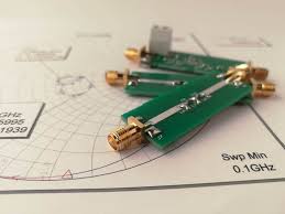
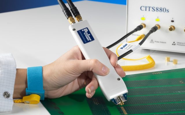
Electrical Validation: From Design Intent to Measured Reality
Design calculations alone are not enough. KKPCB validates controlled impedance PCBs through:
-
Impedance coupons integrated into production panels
-
Time Domain Reflectometry (TDR) testing for every impedance-controlled order
-
Correlation of measured impedance with simulation targets
This verification process ensures that the manufactured PCB meets real-world electrical performance requirements, not just theoretical expectations.
Applications That Depend on Controlled Impedance PCB Architectures
Controlled impedance PCB solutions from KKPCB support a wide range of high-speed applications, including:
-
High-speed computing and data center infrastructure
-
5G and wireless RF transceiver modules
-
Automotive radar and ADAS systems
-
Aerospace and satellite communication platforms
-
Industrial automation and precision control electronics
Each application presents unique challenges in signal integrity, EMI, and manufacturability, all addressed through tailored impedance control strategies.
Conclusion
Building reliable high-speed electronics requires more than fast components—it demands controlled impedance PCB architectures engineered with precision, validated through measurement, and manufactured with discipline.
By combining stackup engineering, material science, fabrication control, and in-house TDR validation, KKPCB delivers controlled impedance PCBs that enable stable signal integrity, predictable performance, and long-term reliability in the most demanding high-speed and RF systems.
