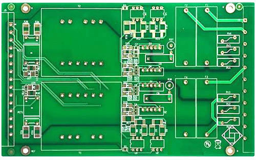
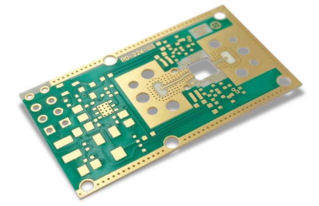
A Double Layer HF PCB is one of the most efficient and cost-optimized architectures for high-frequency designs requiring low-loss transmission, tight impedance control, and stable RF performance up to microwave and lower mmWave ranges. Compared with complex multilayer structures, the Double Layer HF PCB offers a cleaner electromagnetic environment, reduced dielectric loading, and minimized stackup variability—making it ideal for RF front-ends, antenna modules, radar sensors, and IoT communication hardware.
The combination of a simple structure and high-frequency performance makes Double Layer HF PCB technology fundamental for compact, cost-sensitive RF devices that still demand excellent signal integrity.
1. Why Double Layer HF PCB Matters for High-Frequency Designs
High-frequency circuits rely heavily on predictable electromagnetic behavior. The Double Layer HF PCB eliminates many internal dielectric interactions found in thicker stacks. Its advantages include:
• Lower dielectric loss due to reduced material thickness
• Fewer internal interfaces that cause signal scattering
• More stable impedance across wide frequency ranges
• Lower radiation loss thanks to optimized microstrip geometry
• Reduced mode conversion and minimized coupling between RF paths
Because only two layers are involved, the RF designer can precisely control copper geometry, substrate height, and ground return paths—critical for high-frequency PCB performance.
2. Low-Loss HF Materials Improve RF Signal Quality
To maximize performance, Double Layer HF PCBs are typically built using low-loss dielectric materials such as:
• Rogers RO4350B
• Rogers RO4003C
• RT/duroid 5880
• Taconic TLY Series
• Megtron-series HF laminates
These materials provide:
• Low dissipation factor (Df) for clean RF transmission
• Stable dielectric constant (Dk) for predictable impedance
• Low moisture absorption
• High thermal stability for power-handling RF circuits
The result is a Double Layer HF PCB with excellent low-loss behavior essential for filters, couplers, LNAs, PAs, and RF front-end boards.
3. Transmission-Line Engineering for Double Layer HF PCB
Because the Double Layer HF PCB uses a single signal layer and a single ground layer, it is ideal for microstrip and grounded coplanar waveguide (GCPW) routing.
Microstrip advantages:
• Low dielectric loading
• Predictable impedance
• Simplified modeling
GCPW advantages:
• Better isolation
• Lower radiation at high GHz
• Reduced sensitivity to manufacturing tolerance
• Superior confinement of electromagnetic fields
Both structures benefit from stable dielectric materials. This is why the Double Layer HF PCB is commonly used for 2.4 GHz, 5.8 GHz, 24 GHz, and 60 GHz RF systems.
4. Impedance Control Precision in Double Layer HF PCB
Impedance is the backbone of RF PCB engineering. A Double Layer HF PCB simplifies impedance design by reducing stackup variables.
Key factors influencing impedance control include:
• Dielectric height (H)
• Trace width (W)
• Copper thickness (T)
• Dielectric constant (Dk)
• Solder mask interaction
Using a Double Layer HF PCB ensures more stable impedance because the ground reference plane is directly beneath the RF layer, minimizing unexpected field interactions.
For antennas, matching networks, and Wilkinson dividers, this structural simplicity dramatically improves tuning efficiency and bandwidth repeatability.
5. Thermal and Power Handling Advantages
Double Layer HF PCBs dissipate RF heat more efficiently due to:
• Shorter thermal conduction paths
• Direct ground-plane access
• Reduced internal resin heating
• Improved copper-to-ground thermal transfer
This makes them suitable for:
• 2–10 W RF power amplifiers
• Automotive radar front-ends
• Outdoor base-station submodules
• High-temperature IoT transmitters
When paired with low-Df substrates, the board achieves both thermal stability and superior long-term reliability.
6. Application Domains for Double Layer HF PCB
The Double Layer HF PCB architecture is widely deployed in:
• Antenna boards and matching networks
• Wi-Fi, BT, Zigbee RF modules
• GNSS antennas and LNA boards
• 24 GHz and 60 GHz radar modules
• RF measurement tools
• Microwave filters and couplers
• IoT/LPWAN transceiver boards
• Compact RF front-end units
Every domain benefits from predictable impedance, low dielectric loss, and simplified manufacturing.
Conclusion
The Double Layer HF PCB remains one of the most effective solutions for building stable, low-loss, and cost-efficient high-frequency electronic systems. Its structure delivers tight impedance control, predictable RF behavior, and excellent thermal performance—while maintaining high manufacturability.
For RF designers building next-generation wireless modules, radar nodes, or compact antenna systems, the Double Layer HF PCB offers an optimal balance between engineering performance and total system cost.
