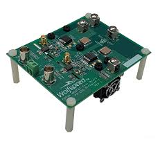
Silicon Carbide (SiC) PCBs are rapidly becoming essential for advanced power electronics, electric vehicles, aerospace systems, and industrial automation due to their ability to operate at higher temperatures, voltages, and frequencies than traditional FR-4 or standard ceramic substrates. SiC PCBs integrate wide-bandgap semiconductor technology directly with optimized thermal and electrical performance to support next-generation applications.
1. Material Science and Properties of SiC PCB
Silicon Carbide substrates are used for PCBs in high-power and high-temperature electronics because of their unique properties:
-
High Thermal Conductivity (≈ 300 W/m·K) – effectively dissipates heat from power semiconductors
-
Wide Bandgap (≈ 3.2 eV) – supports high-voltage operation and reduces leakage current
-
High Dielectric Strength (> 10 kV/mm) – ensures electrical isolation under extreme conditions
-
Mechanical Stability – maintains dimensional accuracy under thermal cycling
-
Low Thermal Expansion (CTE ≈ 4–5 ppm/°C) – reduces stress on solder joints
These characteristics make SiC PCBs ideal for power modules, inverters, DC-DC converters, and high-frequency switching circuits.
2. Thermal Management in SiC PCB
High-power SiC devices generate significant heat. PCB design must include:
-
Thick copper layers or heavy copper plating for power planes
-
Thermal vias to transfer heat from top components to heatsinks or base layers
-
High-thermal-conductivity ceramic cores (AlN, SiC composite)
-
Optimized pad and trace placement to reduce thermal hotspots
Effective thermal management ensures long-term reliability and continuous high-power operation.
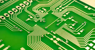
3. Stackup and High-Voltage Design
SiC PCBs often require multi-layer ceramic or hybrid metal-core stackups:
-
Top layer: Component pads and high-current traces
-
Inner layers: Power and ground planes with low impedance
-
Bottom layer: Thermal conduction layer or heat-spreading plane
Design must ensure high-voltage isolation between traces and planes, particularly for automotive and aerospace applications.
4. Reliability and High-Temperature Operation
SiC PCBs are engineered for environments up to 300°C or higher. Key engineering practices include:
-
Selecting high-Tg, low-CTE laminates or ceramics
-
Using sintered silver or gold metallization for high-temperature soldering
-
Minimizing thermal expansion mismatch between substrate and SiC devices
-
Implementing robust EMI/EMC shielding for sensitive circuits
These measures ensure stable operation under extreme thermal and electrical stress.
5. Applications of SiC PCB
SiC PCB is increasingly applied in:
-
Electric vehicles (EVs) – inverters, onboard chargers, DC-DC converters
-
Renewable energy systems – solar inverters, wind turbine converters
-
Aerospace & defense electronics – high-voltage power modules, radar electronics
-
Industrial automation – high-frequency switching, high-power motor drives
-
Advanced robotics – high-efficiency motor controllers and power electronics
In each scenario, SiC PCB ensures high efficiency, reduced energy loss, and reliability under high-stress conditions.
6. Engineering Summary
SiC PCBs are a cornerstone for high-power, high-temperature, and high-frequency electronics. By integrating:
-
Advanced SiC material properties
-
Optimized stackup and thermal management
-
High-voltage isolation and EMI mitigation
-
Robust metallization for high-temperature soldering
engineers can develop reliable, efficient, and compact power systems for automotive, aerospace, industrial, and renewable energy applications.
KKPCB provides full engineering, prototyping, and manufacturing solutions for SiC PCB, delivering high-quality, high-performance boards for next-generation electronics.
