Modern data center networks depend on multi-gigabit signal transmission, low-latency switching, and phase-coherent high-speed channels. As switching fabrics migrate from 25G/40G toward 100G/200G/400G architectures, even micro-scale distortions in dielectric properties or copper structures can degrade eye diagrams, reduce SNR, and trigger packet loss.
This is why Low Loss PCB stackups—built with engineered dielectric materials and ultra-controlled impedance structures—have become the backbone of next-generation high-speed interconnects.
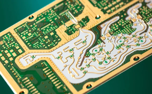
At KKPCB, we design phase-stable, low-loss PCB architectures optimized specifically for switches, routers, storage fabrics, accelerator boards, AI servers, and HPC clusters where routing precision determines system throughput.
Why Low Loss PCB Stackups Are Essential for Multi-Gigabit Integrity
Multi-gigabit networks push differential pairs to operate in the 10–112 Gbps range, where dielectric performance defines channel quality.
Key parameters include:
-
Dk Stability (Dielectric Constant Uniformity) → Ensures predictable impedance
-
Df Reduction (Dissipation Factor / Loss Tangent) → Minimizes insertion loss
-
Phase Stability → Maintains time alignment across differential pairs
-
Copper Roughness Control → Reduces skin-effect loss at high frequencies
-
Low Mode Conversion → Prevents differential-to-common-mode distortion
If any parameter drifts, high-speed routes lose synchronization, degrading link quality and limiting the achievable baud rate.
Low Loss PCB materials such as Megtron 6, Megtron 7, Tachyon 100G, I-Speed, and Nelco SI family maintain consistent high-frequency performance across broad temperatures—making them the preferred foundation for data center networks.
Engineering Principles Behind Phase-Stable Multi-Gigabit Routing
1. Controlled Dielectric Uniformity
A low-loss PCB must maintain ±2% or better dielectric constant uniformity across layers to keep differential impedance stable over long routing distances.
2. Differential Pair Integrity Across Layers
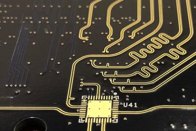
With 20–36 layer server PCBs, transitions introduce skew. KKPCB applies:
-
Layer-to-layer Dk matching
-
Tight copper bonding
-
Optimized glass-weave angle control
-
Back-drilling for stub removal
This ensures consistent propagation delay across multi-layer interconnect paths.
3. Ultra-Low Insertion Loss Material Selection
Using materials with Df < 0.003 ensures clean high-frequency transmission up to mmWave domains.
This is crucial for PCIe Gen5/Gen6, 100G SerDes, and PAM4 modulation schemes.
4. Phase-Coherent High-Speed Channels
Phase stability is critical in spine–leaf switches and AI cluster backplanes where:
-
Synchronous links must remain aligned
-
Skew margins shrink as baud rates climb
-
Equalization budgets become constrained
KKPCB ensures ≤1 ps/in phase variation through precision lamination and uniform dielectric compression.
Low Loss PCB Stackup Techniques Used by KKPCB
Optimized Stackup Architecture
-
Symmetrical builds
-
Balanced resin distribution
-
Low-profile copper (HVLP/EDLP)
-
Controlled z-axis dielectric thickness
-
Impedance-matched reference planes
Advanced High-Speed Manufacturing Controls
-
Automated optical layer alignment (<10 µm)
-
Pressed stackup verification using Z-axis metrology
-
Backdrill accuracy <75 µm
-
Surface roughness control for ultra-low loss routing
-
Exacting trace width/spacing tolerances for 100G+ channels
Thermal & Frequency Stability Modeling
Using HFSS, SiSoft, and ADS, KKPCB simulates:
-
Eye diagram performance
-
Skew accumulation
-
Frequency-dependent insertion loss
-
Crosstalk across dense routing
-
Differential-to-common-mode conversion
This ensures that every PCB design supports predictable multi-gigabit behavior.
Applications in High-Speed Data Center Networks
Low Loss PCB stackups from KKPCB are deployed in:
-
100G/200G/400G/800G switches
-
AI accelerator clusters
-
Ethernet PHY & SerDes cards
-
Storage backplanes (NVMe, SAS, PCIe Gen5/6)
-
Optical transceiver modules
-
Server motherboards & compute blades
Every system benefits from improved channel integrity, reduced BER, and lower power consumption for equalization.
Conclusion
Achieving phase-stable, multi-gigabit routing requires far more than standard PCB manufacturing.
Data center networks demand low-loss dielectric materials, precision stackup design, controlled copper structures, and deep 啊客户不是 engineering expertise. KKPCB delivers optimized low-loss PCB platforms that ensure:
-
Consistent phase alignment
-
Ultra-low insertion loss
-
Low crosstalk
-
Stable impedance control
-
Reliable multi-gigabit throughput
These high-performance PCBs form the critical foundation for the future of high-speed data center networks.
