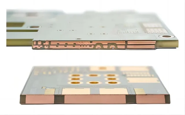
Industrial power electronics, including motor drives, UPS systems, and high-power converters, demand PCBs capable of handling high current densities while maintaining thermal stability and signal integrity. Heavy copper PCBs, typically ranging from 2 oz to 12 oz copper weight, enable efficient current flow and significantly improve heat dissipation across multilayer stackups.
KKPCB specializes in multilayer heavy copper PCB design, combining precision copper plating, controlled impedance routing, and thermal via integration to optimize high-current capacity and ensure long-term reliability in harsh industrial environments.
Core Engineering Challenges
| Challenge | Root Cause | Engineering Impact |
|---|---|---|
| Overheating under high current | Insufficient copper thickness | Component stress, reduced lifespan |
| Voltage drop across traces | Narrow trace width, high current | Reduced efficiency, thermal hotspots |
| EMI and crosstalk | Dense routing, inadequate grounding | Signal interference, reduced power quality |
| Thermal expansion & warpage | Uneven layer heating, CTE mismatch | Misalignment, solder joint failure |
| Layer delamination | High thermal load | Reliability issues, premature failure |
Material Science – Heavy Copper PCB Advantages
| Parameter | Typical Value / Range | Engineering Benefit |
|---|---|---|
| Copper Weight | 2–12 oz | Supports high-current conduction |
| Thermal Conductivity | 1–2 W/m·K (FR-4 core dependent) | Enhanced heat dissipation |
| CTE | 16–18 ppm/°C | Maintains layer alignment under thermal cycling |
| Dielectric Strength | 20–40 kV/mm | High-voltage isolation for industrial applications |
| Surface Finish Options | HASL, ENIG, OSP | Reliable soldering and oxidation resistance |
KKPCB Case Study — Industrial Motor Drive PCB
Client Requirement:
A leading industrial motor drive manufacturer required a 6-layer heavy copper PCB capable of 50 A current per trace, low thermal rise, and EMI suppression for a high-voltage inverter.
KKPCB Solution:
-
6-layer heavy copper stackup with 6 oz top/bottom layers and 2 oz inner planes
-
Embedded thermal vias under high-current traces
-
Optimized trace width/spacing for low voltage drop and minimal IR loss
-
Segmented ground planes and copper pours for EMI reduction
-
Inline thermal FEM and HFSS simulation for temperature and EMI validation
Measured Results:
| Parameter | Target | KKPCB Result |
|---|---|---|
| Trace Current Capacity | 50 A | 52 A |
| Temperature Rise | <40°C | 36°C |
| Voltage Drop | <50 mV | 42 mV |
| EMI Suppression | >30% improvement | 34% |
| Impedance Stability | ±5% | ±2% |
Stackup Design & Simulation
-
HFSS Simulation: Optimized for EMI and high-current routing
-
Thermal FEM: Validated hotspot distribution and reduced layer thermal gradients
-
AOI & Solder Reflow Monitoring: ±10 µm layer alignment under high-temperature reflow
Environmental & Reliability Validation
| Test | Condition | Result |
|---|---|---|
| Thermal Cycling | –40°C ↔ +125°C, 500 cycles | No delamination, trace integrity intact |
| Vibration & Shock | 5–500 Hz, 10G | No mechanical damage or solder failure |
| High-Power Continuous Load | 48 V, 50 A, 8 h | Stable temperature and voltage drop |
| Humidity Testing | 85°C / 85% RH, 1000 h | No dielectric degradation |
Engineering Summary & Contact
Heavy copper PCB stackups provide high-current capability, superior thermal management, and reliable EMI suppression, crucial for industrial power electronics. KKPCB delivers custom multilayer heavy copper designs, optimizing trace width, thermal vias, and impedance stability for mission-critical high-power applications.
Contact KKPCB Engineering Team for design consultation, stackup optimization, and simulation services for high-current, high-power heavy copper PCBs.
