Satellite communication payloads demand high-frequency RF stability, minimal insertion loss, and optimized power efficiency across densely packed multilayer PCBs. Signal integrity degradation, EMI coupling, or thermal hotspots can compromise link margin, telemetry accuracy, and antenna performance.
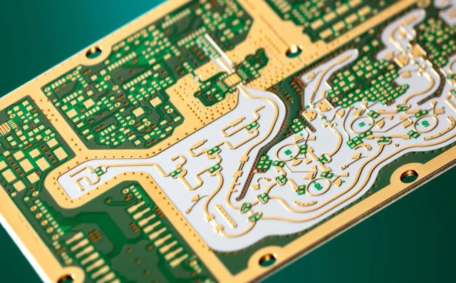
Low loss PCB materials, such as ceramic-reinforced laminates or PTFE-based RF substrates, provide stable dielectric constant (Dk) and low dissipation factor (Df) even under extreme thermal, vacuum, and radiation conditions. KKPCB employs precision lamination, impedance-controlled routing, and EMI mitigation strategies to ensure phase-stable, low-loss signal chains for satellite transceivers, phased-array antennas, and high-power RF amplifiers.
Core Engineering Challenges
| Challenge | Root Cause | Engineering Impact |
|---|---|---|
| Insertion loss at high GHz | Surface roughness, dielectric dissipation | Reduced RF gain, lowered uplink/downlink margin |
| Thermal hotspots in dense layers | Poor heat dissipation | Local impedance drift, phase misalignment |
| EMI coupling in multilayer traces | Tight spacing, insufficient ground planes | Crosstalk, signal distortion |
| Phase instability under vacuum | Lamination tolerance, resin flow | Beamforming errors, degraded telemetry accuracy |
| Long-term reliability | Thermal cycling, radiation | Material degradation, signal attenuation over mission |
Material Science – Low Loss PCB Advantages
| Parameter | Typical Value | Engineering Benefit |
|---|---|---|
| Dk | 3.0 – 9.8 | Stable impedance across multilayer RF stackups |
| Df | 0.001–0.004 | Minimizes insertion loss and preserves signal integrity |
| Thermal Conductivity | 0.5–2.5 W/m·K | Efficient heat spreading in high-power layers |
| CTE | 6–17 ppm/°C | Maintains multilayer alignment under thermal stress |
| Moisture Absorption | <0.05% | Preserves dielectric stability in high-humidity environments |
Compared with standard FR-4, low loss PCB substrates significantly reduce insertion loss, enhance RF power efficiency, and maintain phase-stable performance in high-frequency satellite payloads.
KKPCB Case Study — Satellite Ku/Ka-Band Transceiver PCB
Client Context:
A leading aerospace OEM required a 6-layer low loss PCB for a Ku/Ka-band transceiver operating in geostationary satellites. Prior designs experienced ~5% impedance variation, phase ripple >2°, and EMI-induced cross-channel interference.
KKPCB Solution:
-
Hybrid multilayer low loss PCB stackup (ceramic/PTFE composite)
-
Controlled copper roughness (Ra <0.8 µm)
-
±5 μm dielectric thickness tolerance via precision lamination
-
Embedded calibration traces for inline TDR verification
-
Optimized ground plane segmentation and trace spacing for EMI suppression
Measured Results:
| Parameter | Target | KKPCB Result |
|---|---|---|
| Insertion Loss @20 GHz | <0.35 dB/in | 0.28 dB/in |
| Phase Deviation | <1° | 0.55° |
| Return Loss (S11) | < –15 dB | –17.2 dB |
| EMI Reduction | >30% | 33% |
| Impedance Variation | ±5% | ±2% |
Stackup Design & RF Simulation
-
HFSS Modeling: Optimized microstrip/stripline impedance, minimized interlayer coupling
-
ADS & TDR: Verified phase linearity <0.6° across high-frequency channels
-
Thermal FEM: Hotspot reduction of 5–6°C in high-power layers
-
AOI & Solder Reflow Monitoring: ±10 µm alignment across multilayers
Environmental & Reliability Validation
| Test | Condition | Result |
|---|---|---|
| Thermal Cycling | –55°C ↔ +125°C, 1000 cycles | Phase deviation <0.6°, no delamination |
| Vibration & Shock | 5–500 Hz, 10G | No trace or solder failures |
| Vacuum Outgassing | <0.1% TML | Material stable in space environment |
| High-Power RF Operation | Continuous 28–40 GHz | Minimal insertion loss increase (<0.02 dB) |
| Solder Reflow | 260°C ×3 cycles | Stackup alignment maintained |
Engineering Summary & Contact
Low loss PCB designs provide reduced insertion loss, enhanced RF power efficiency, and phase-stable signal transmission for satellite communication payloads. KKPCB’s precision stackups, EMI mitigation, and thermal management solutions ensure long-term reliability for Ku/Ka-band transceivers, phased-array antennas, and high-power RF modules.
Contact KKPCB Engineering Team for design consultation, multilayer low loss PCB optimization, and high-frequency RF performance verification for your next-generation satellite communication project.
