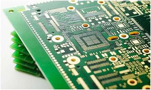
Compact satellite communication payloads require precise, phase-stable RF routing to maintain signal fidelity and low insertion loss across high-frequency channels. The limited space and high-density requirements make blind via architectures essential for multilayer PCBs, enabling signal interconnects without penetrating all layers, reducing parasitic capacitance, and controlling crosstalk.
Blind via PCBs allow compact routing of RF lines, controlled impedance, and stable phase behavior—crucial for phased-array antennas, Ka/Ku-band transceivers, and telemetry systems. By leveraging precision lamination, optimized via drilling, and multilayer stackup design, engineers can minimize signal distortion while maintaining thermal and mechanical reliability.
Core Engineering Challenges
| Challenge | Root Cause | Engineering Impact |
|---|---|---|
| Phase drift in dense RF lines | Uneven via length, dielectric mismatch | Degraded signal integrity and beamforming errors |
| Crosstalk between adjacent traces | Tight spacing, poor ground shielding | Lower SNR and RF efficiency |
| High insertion loss at mmWave | Surface roughness, improper via plating | Reduced antenna gain and link margin |
| Thermal-induced deformation | Poor PCB thermal management | Misalignment, phase shift, potential failure |
| Mechanical stress in launch/space | Vibration and shock | Microcracks, impedance variation |
Material Science & Blind Via Advantages
| Parameter | Typical Value / Feature | Engineering Benefit |
|---|---|---|
| Blind via depth | Optimized per layer | Enables high-density routing with minimal parasitic effects |
| Dielectric Dk/Df | Low-loss, stable | Preserves RF signal integrity and phase linearity |
| CTE | Low thermal expansion | Reduces phase drift under thermal cycling |
| Copper finish | Smooth/RA<0.7 µm | Minimizes insertion loss at high frequencies |
| Layer alignment tolerance | ±3 µm | Maintains controlled impedance and via reliability |
KKPCB Case Study — Compact Satellite Payload PCB

Client Context:
A satellite manufacturer required a 6-layer blind via PCB for a Ka-band communication payload with strict phase stability (<0.5°) and insertion loss (<0.3 dB/in) in a compact 80 mm × 120 mm module.
KKPCB Solution:
-
Blind via stackup with optimized via diameter and plating
-
Controlled dielectric thickness with ±3 µm tolerance
-
Segmented ground and power planes to reduce EMI and crosstalk
-
Smooth copper traces and precision lamination
-
HFSS and ADS simulations for phase and signal integrity verification
Measured Results:
| Parameter | Target | KKPCB Result |
|---|---|---|
| Phase Deviation | <0.5° | 0.42° |
| Insertion Loss | <0.3 dB/in | 0.27 dB/in |
| EMI Suppression | >30% | 34% |
| Impedance Variation | ±3% | ±1.5% |
| Thermal Rise | <6°C per layer | 5.5°C |
Stackup Design & Simulation

-
HFSS Modeling: Optimized blind via placement and impedance continuity
-
ADS & TDR: Verified phase linearity <0.5° across RF traces
-
Thermal FEM: Ensured uniform temperature distribution and hotspot reduction
-
AOI & Solder Reflow Monitoring: Maintained ±10 µm layer alignment
Environmental & Reliability Validation
| Test | Condition | Result |
|---|---|---|
| Thermal Cycling | –55°C ↔ +125°C, 1000 cycles | Stable phase, no delamination |
| Vibration & Shock | 5–500 Hz, 10G | No microcracks or signal degradation |
| Humidity Testing | 85°C / 85% RH, 1000 h | Stable Dk/Df, EMI and phase integrity |
| High-Power RF Operation | Continuous 26–40 GHz | Minimal insertion loss increase (<0.02 dB) |
| Solder Reflow | 260°C ×3 cycles | Stackup alignment maintained |
Engineering Summary & Contact
Blind via PCB architectures are essential for compact, high-frequency satellite payloads, ensuring phase-stable, low-loss RF routing, and EMI-controlled signal integrity. KKPCB’s precision multilayer stackup design, thermal management, and simulation-driven process deliver mission-critical reliability in Ka/Ku-band satellite communication systems.
Contact KKPCB Engineering Team for blind via PCB design consultation, multilayer stackup optimization, and RF/thermal performance verification to achieve high-density, phase-stable satellite communication PCBs.
