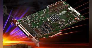
Radar PCB: Design Principles, Materials, Manufacturing Challenges & Key Applications
High-speed PCBs stand at the top of modern circuit-board technology, spanning digital high-speed, mixed-signal, and RF/microwave categories. Among these, RF and microwave PCBs operate at the highest frequencies, making them essential for advanced applications—especially RADAR (Radio Detection and Ranging).
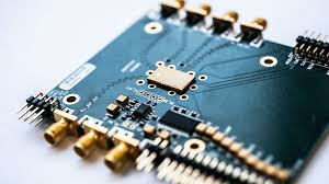
Because Radar PCBs frequently host a mix of RF and high-speed digital signals, they require the same stringent design discipline as mixed-signal and microwave boards. Their combination of extreme frequencies, tight tolerances, and reliability demands makes Radar PCBs one of the most complex PCB types to design and manufacture.
What Are Radar PCBs?
Radar technology detects objects and measures distance, velocity, and direction using radio waves. A radar system transmits radio signals through an antenna, receives the reflected signals, and processes the timing, phase, or frequency shift.
Radar PCBs must guide these RF signals from antenna to processor with minimal attenuation and distortion. Operating in frequency bands typically ranging from 1 GHz to 77 GHz, Radar PCBs face severe challenges:
-
High sensitivity to crosstalk & electromagnetic interference
-
Significant signal reflection & loss at high frequencies
-
Skin-effect induced losses
-
Strict signal integrity & EMC requirements
-
Demands for aerospace-grade reliability
These factors make radar PCB design an advanced engineering discipline requiring precise control over material selection, stack-up, impedance, and manufacturing tolerances.
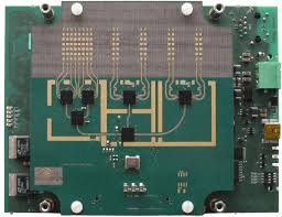
Design Considerations for Radar PCBs
1. Selecting the Right Layer Stack
Radar PCBs often combine RF, analog, and digital domains. This requires:
-
Multiple ground planes
-
Separation of RF ground and digital ground
-
Controlled-impedance structures
-
Hybrid material stack-ups (e.g., FR4 + PTFE)
The layer stack directly influences trace characteristics, manufacturability, and thermal behavior.
2. Selecting the Right Materials
Standard FR4 fails above ~1–2 GHz unless trace lengths are extremely short. Radar PCBs require low-loss laminates, evaluated through:
-
Dielectric constant (Dk) – controls impedance
-
Dissipation factor (Df) – determines signal attenuation
-
Thermal stability
-
Coefficient of thermal expansion (CTE)
Lower Df = lower attenuation = better high-frequency performance.
3. Impedance & Length Matching
To preserve timing and signal integrity:
-
RF lines require precise 50-ohm characteristic impedance
-
Digital high-speed interfaces use controlled differential impedance
-
Multichannel digital signals require length matching to prevent skew
-
RF trace impedance must be maintained across the entire routing path
4. Proper Ground Shielding
High-speed PCB success depends heavily on return-path integrity:
-
Use via fences and ground stitching
-
Maintain continuous ground beneath RF traces
-
Avoid ground plane under antennas or antenna modules
(otherwise antenna reception is severely degraded)
Effective shielding mitigates EM coupling, improves SI/PI/EMC, and reduces reflections.
Materials Commonly Used in Radar PCBs
RO4350B
-
Dk = 3.48
-
Df = 0.0037
-
Low-cost performance, easy fabrication
-
Ideal for hybrid stacks with FR4
RO3003
-
Dk = 3.00
-
Df = 0.0013
-
Ultra-low loss
-
Frequently used for high-end Radar and mmWave PCBs
Astra MT77 (Isola)
-
Dk = 3.00
-
Df = 0.0017
-
Exceptional electrical/thermal stability
-
Excellent for automotive radar (77 GHz)
Taconic RF-35
-
Dk = 3.5
-
Df = 0.0018
-
Preferred for FMCW and Doppler radar
-
Reliable and cost-effective
These laminates define RF performance, manufacturability, long-term stability, and cost.
Applications of Radar PCBs
Different radar systems require different PCB architectures:
• FMCW Radar
-
Measures range & velocity
-
Used in altimeters, automotive radar
• Doppler Radar
-
Velocity measurement via Doppler shift
-
Used in motion detectors, security systems
• Pulsed Radar
-
Long-range detection using short bursts
-
Used in surveillance & military radar
• Phased Array Radar
-
Electronic beam steering
-
Used in 5G base stations, defense systems
• Synthetic Aperture Radar (SAR)
-
Generates high-resolution Earth imaging
-
Used in satellites and mapping
• MIMO Radar
-
Multi-antenna radar for high resolution
-
Widely used in autonomous vehicles
Conclusion
Radar PCB design requires expertise in RF engineering, electromagnetic simulation, material science, and advanced PCB layout practices. Every design needs careful coordination between PCB engineers, RF designers, and manufacturing partners capable of handling precise, low-loss microwave materials.
For new engineers stepping into the world of radar technology, ongoing learning combined with partnering with a seasoned Radar PCB manufacturer such as KKPCB can significantly streamline development, reduce design risks, and elevate project success rates.
