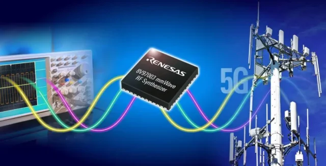
As 5G technology expands into millimeter-wave frequency bands, PCB performance becomes a critical factor in system reliability and signal quality. The 5G mmWave PCB is engineered to support ultra-high frequencies, extremely short wavelengths, and strict signal integrity requirements that far exceed conventional RF designs.
A professionally manufactured 5G mmWave PCB enables stable and repeatable performance in advanced communication systems.
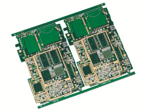
What Is a 5G mmWave PCB?
A 5G mmWave PCB is a high-frequency printed circuit board designed to operate in the millimeter-wave spectrum, typically above 24 GHz. These PCBs are optimized for:
-
Ultra-low signal loss
-
Precise impedance control
-
Tight dimensional accuracy
They form the backbone of 5G mmWave communication hardware.
Why 5G mmWave PCB Design Is Challenging
At mmWave frequencies, even minor design deviations can cause:
-
Severe signal attenuation
-
Impedance mismatch and reflections
-
Phase and timing errors
5G mmWave PCBs must be engineered with extreme precision.
Low-Loss Materials for 5G mmWave PCBs
Material selection is critical. Common choices include:
-
Rogers RO3003 / RO4003 series
-
PTFE-based laminates
-
Hybrid RF stackups
Low dielectric loss ensures minimal attenuation at mmWave frequencies.
Controlled Impedance and Transmission Line Accuracy
5G mmWave PCBs require:
-
Highly accurate trace geometry
-
Stable dielectric thickness
-
Tight impedance tolerance
Precise impedance control ensures consistent signal behavior across channels.
Stackup Design for mmWave Performance

Optimized stackups include:
-
Dedicated mmWave signal layers
-
Continuous reference planes
-
Isolation between RF and digital sections
Proper stackup design reduces crosstalk and EMI.
Via Design and Transition Optimization
Vias become significant discontinuities at mmWave frequencies. Effective solutions include:
-
Short via lengths
-
Back-drilling to remove stubs
-
Grounded via fences near RF traces
These techniques reduce parasitic effects.
Manufacturing Precision and Process Control
Fabricating 5G mmWave PCBs requires:
-
Ultra-fine line etching
-
Precise lamination control
-
RF impedance and loss testing
Strict process control ensures repeatable performance.
Typical Applications of 5G mmWave PCBs
5G mmWave PCBs are widely used in:
-
5G base stations and small cells
-
mmWave RF front-end modules
-
Phased array antennas
-
Automotive and industrial mmWave systems
Each application demands ultra-high-frequency stability.
Choosing a 5G mmWave PCB Manufacturer
When selecting a 5G mmWave PCB supplier, look for:
-
Proven mmWave PCB experience
-
Advanced material handling capability
-
Controlled impedance and RF testing support
-
Engineering collaboration from design to production
An experienced partner ensures successful mmWave deployment.
Conclusion
The 5G mmWave PCB is a critical enabler of next-generation wireless communication. Through low-loss materials, precise impedance control, and advanced manufacturing processes, these PCBs deliver reliable performance at millimeter-wave frequencies.
Working with an experienced 5G mmWave PCB manufacturer ensures your designs meet the demanding requirements of modern 5G systems.
