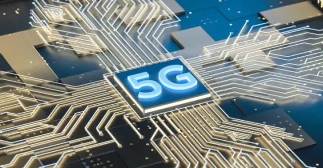
A 5G IC Test PCB is a specialized printed circuit board used to validate 5G baseband ICs, RF transceivers, power amplifiers, and mmWave front-end modules. As 5G technology operates at sub-6 GHz and millimeter-wave frequencies, the performance requirements for test PCBs are significantly higher than those for conventional IC testing.
5G IC test PCBs play a critical role in Automated Test Equipment (ATE), load boards, probe card interfaces, and device characterization platforms, where signal integrity, impedance accuracy, and repeatability directly affect test results.
Key Design Challenges in 5G IC Test PCBs
1. High-Frequency Signal Integrity
5G signals are highly sensitive to impedance mismatch, insertion loss, and reflection. A 5G IC test PCB must use precise controlled impedance routing and low-loss materials to ensure accurate RF and digital signal transmission.
2. mmWave Routing and Layout Complexity
At millimeter-wave frequencies, even minor layout deviations can cause significant signal degradation. Optimized trace geometry, via transitions, and RF grounding structures are essential for reliable 5G IC testing.
3. RF and Digital Signal Isolation
5G ICs integrate RF, analog, and high-speed digital blocks. Effective isolation between these domains on the test PCB is required to minimize noise coupling and interference.
4. Power Integrity for 5G ICs
5G ICs often operate under dynamic power conditions. Stable power delivery with low-inductance planes and dense decoupling is critical to prevent test variability.
Structural Features of 5G IC Test PCBs
A high-quality 5G IC test PCB typically incorporates:
-
Controlled impedance transmission lines for RF and high-speed digital signals
-
Low-loss and low-Dk materials suitable for sub-6 GHz and mmWave applications
-
Multilayer PCB stackups separating RF, digital, and power domains
-
Microvias, blind vias, and via-in-pad structures to minimize parasitic effects
-
High-density routing to support high pin count 5G IC packages
These features ensure stable, repeatable, and accurate 5G IC test performance.
Applications of 5G IC Test PCBs
5G IC test PCBs are widely used in:
-
5G RF transceiver and baseband IC testing
-
mmWave front-end module validation
-
ATE load boards for 5G devices
-
5G SoC and RFIC characterization
-
Wireless infrastructure and automotive 5G IC testing
Accurate test PCBs are essential to meeting 5G performance and compliance standards.
Manufacturing Requirements for 5G IC Test PCBs
Producing reliable 5G IC test PCBs requires:
-
Tight impedance tolerance and trace geometry control
-
Advanced multilayer lamination and precise registration
-
High-frequency material handling expertise
-
RF performance testing and impedance verification
-
Support for prototypes, small batch, and production volumes
An experienced manufacturer ensures high yield, consistent RF performance, and fast turnaround for semiconductor testing needs.
Conclusion
A 5G IC Test PCB is a critical component in the development and validation of next-generation wireless integrated circuits. By combining controlled impedance design, low-loss materials, advanced multilayer construction, and robust power integrity, these PCBs enable accurate, repeatable, and reliable 5G IC testing.
Partnering with a trusted 5G IC test PCB manufacturer helps semiconductor companies reduce test risk, accelerate qualification, and achieve consistent test results from engineering validation through mass production.
