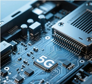
A 5G IC Test PCB is a specialized high-frequency semiconductor test PCB engineered to validate 5G communication ICs, including RF front-end modules, mmWave transceivers, and high-speed baseband processors. With 5G devices operating at gigahertz frequencies, maintaining signal integrity, impedance control, and low-loss transmission is essential for accurate testing.
These test PCBs form the interface between 5G ICs and Automated Test Equipment (ATE), enabling precise evaluation of high-frequency performance, power delivery, and thermal stability.
Key Design Considerations for 5G IC Test PCBs
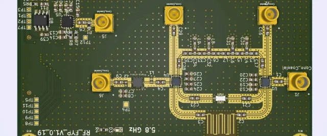
1. Controlled Impedance and High-Frequency Routing
5G ICs operate at high RF and mmWave frequencies, requiring precise controlled impedance routing, trace length matching, and minimal crosstalk to preserve signal integrity during testing.
2. Low-Loss PCB Materials
Materials such as RO4003, Rogers RT/duroid, PTFE laminates, and hybrid stackups reduce high-frequency signal loss, ensuring accurate RF measurements.
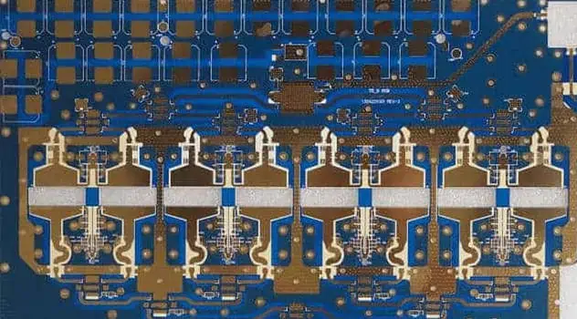
3. High Pin Count and HDI Technology
Modern 5G IC packages often feature hundreds of pins, requiring HDI routing, microvias, fine-line traces, and multilayer structures to maintain reliable electrical access.
4. Thermal and Mechanical Stability
Accurate testing requires PCBs that maintain flatness, dimensional stability, and mechanical reliability under thermal stress from extended testing or elevated RF power conditions.
5. Robust Power Delivery Network (PDN)
A well-designed PDN with low-impedance planes and decoupling ensures consistent voltage supply and minimizes noise, critical for high-frequency IC accuracy.
Applications of 5G IC Test PCBs
5G IC test PCBs are widely used in:
-
5G RF transceiver and front-end module testing
-
mmWave IC characterization and validation
-
High-speed baseband processor testing
-
Automotive 5G communication IC qualification
-
Industrial and IoT 5G module testing
These applications demand precise high-frequency testing, repeatable results, and reliable signal integrity.
Manufacturing Requirements for 5G IC Test PCBs
Producing high-quality 5G IC test boards requires:
-
Multilayer HDI PCB fabrication
-
Microvia and fine-line etching technology
-
Controlled impedance verification
-
Low-loss, high-frequency laminates
-
Prototype, small batch, and volume production support
Strict process control ensures reliable performance across multiple test cycles and production volumes.
Why 5G IC Test PCB Quality Matters
Poor-quality 5G IC test PCBs can cause:
-
Signal degradation and impedance mismatches
-
Inaccurate RF measurement and reduced test yield
-
Increased debugging and validation time
-
Higher operational costs and equipment wear
A high-quality 5G IC Test PCB guarantees accurate testing, reliable RF performance, and efficient ATE validation.
Conclusion
The 5G IC Test PCB is an essential tool for validating high-frequency 5G communication ICs, ensuring reliable RF and mmWave performance. With controlled impedance, low-loss materials, HDI routing, and robust power delivery, these boards enable precise, repeatable, and high-efficiency testing.
Partnering with an experienced 5G IC test PCB manufacturer ensures fast validation, improved yield, and long-term reliability for next-generation communication devices.
