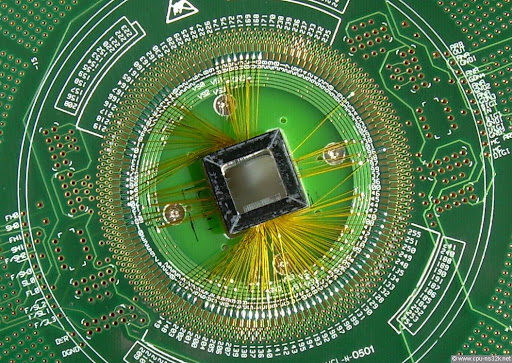
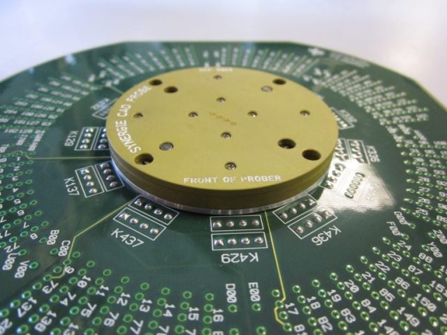
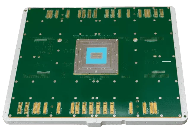
In modern semiconductor manufacturing, wafer-level testing is a critical step to ensure IC functionality, yield, and quality before packaging. Wafer Test PCBs serve as the electrical interface between probe cards and automated test equipment (ATE), enabling accurate signal transmission, high-density connections, and controlled impedance for reliable testing of wafers.
By using high-quality wafer test PCBs, engineers can efficiently validate large numbers of dies, reduce testing errors, and accelerate time-to-market for complex semiconductor devices.
What Is a Wafer Test PCB?
A wafer test PCB is a specialized printed circuit board designed to interface with probe cards and ATE systems. Its main purpose is to:
-
Route high-density signals from IC pads to the testing system
-
Provide stable mechanical support and alignment for probe tips
-
Maintain controlled impedance and low signal loss for high-speed or RF wafers
-
Support repeatable, high-volume wafer-level testing
These PCBs are engineered for accuracy, durability, and high reliability under rigorous test cycles.
Key Features of Wafer Test PCBs
-
High Pin Count Support
Wafer test PCBs can accommodate thousands of connections from modern ICs with dense pad layouts. -
Controlled Impedance
Ensures signal integrity for high-speed and RF testing, minimizing reflections and cross-talk. -
Multilayer Stackups
Enables efficient routing of power, ground, and signal layers while reducing noise and interference. -
Mechanical Precision
Provides accurate alignment for probe cards, preventing pad damage and ensuring consistent test results. -
Thermal and Electrical Reliability
Withstands repeated test cycles and thermal variations during wafer-level burn-in and functional testing.
Materials and Stackup Considerations
Choosing the right materials and stackups is critical for wafer test PCB performance:
-
High-Tg FR-4 – Suitable for general wafer testing with moderate speed signals
-
Low-Loss Laminates – Essential for RF and high-frequency wafer testing
-
Hybrid Stackups – Combines standard FR-4 with high-frequency cores for optimized performance
-
Thermal Management Materials – Maintain mechanical stability during burn-in or high-current testing
Proper material selection ensures both electrical and mechanical reliability.
Applications of Wafer Test PCBs
Wafer test PCBs are widely applied in:
-
Wafer-level functional and parametric testing
-
High-speed digital IC validation
-
RF and mixed-signal semiconductor testing
-
Probe card interfaces for ATE systems
-
Small batch and pilot production IC validation
They play a crucial role in improving yield, reducing test errors, and validating IC designs early in the production process.
Choosing a Wafer Test PCB Manufacturer
When selecting a wafer test PCB supplier, consider:
-
Expertise in high-density, multilayer, and controlled-impedance PCB design
-
Capability for high pin count routing and precise alignment
-
Experience with high-frequency, high-speed, or RF wafer applications
-
Support for prototype, small-batch, and volume production
-
Strict quality control and electrical verification processes
A professional wafer test PCB partner ensures consistent performance, repeatable results, and reduced development risk.
Conclusion
Wafer Test PCBs are a cornerstone of modern semiconductor validation, providing high-density routing, controlled impedance, and mechanical precision for probe card and ATE applications. By partnering with a reliable wafer test PCB manufacturer, engineers can achieve faster design validation, higher yield, and seamless transition from wafer testing to full-scale production.
